


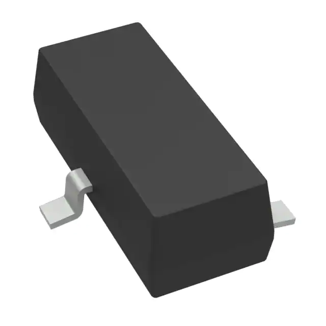
Spot electronic IC chip TL431BIDBZR integrated circuit Voltage References BOM SERVICE RELIABLE SUPPLIER
Both the TL431 and TL432 devices are offered in three grades, with initial tolerances (at 25°C) of 0.5%, 1%, and 2%, for the B, A, and standard grade, respectively. In addition, low output drift versus temperature ensures good stability over the entire temperature range.
The TL43xxC devices are characterized for operation from 0°C to 70°C, the TL43xxI devices are characterized for operation from –40°C to 85°C, and the TL43xxQ devices are characterized for operation from –40°C to 125°C.
Product Attributes
|
TYPE |
DESCRIPTION |
|
Category |
Integrated Circuits (ICs) PMIC - Voltage Reference |
|
Mfr |
Texas Instruments |
|
Mfr |
Texas Instruments |
|
Series |
- |
|
Package |
Tape & Reel (TR) Cut Tape (CT) Digi-Reel® |
|
SPQ |
250T&R |
|
Product Status |
Active |
|
Reference Type |
Shunt |
|
Output Type |
Adjustable |
|
Voltage - Output (Min/Fixed) |
2.495V |
|
Voltage - Output (Max) |
36 V |
|
Current - Output |
100 mA |
|
Tolerance |
±0.5% |
|
Temperature Coefficient |
- |
|
Noise - 0.1Hz to 10Hz |
- |
|
Noise - 10Hz to 10kHz |
- |
|
Voltage - Input |
- |
|
Current - Supply |
- |
|
Current - Cathode |
700 µA |
|
Operating Temperature |
-40°C ~ 85°C (TA) |
|
Mounting Type |
Surface Mount |
|
Package / Case |
TO-236-3, SC-59, SOT-23-3 |
|
Supplier Device Package |
SOT-23-3 |
|
Base Product Number |
TL431 |
Effect
The role of voltage reference chips.
Within the rated operating current range, the accuracy of the reference voltage source device (the deviation of the voltage value, drift, current adjustment rate, and other indicator parameters) is much better than the ordinary more zen regulator diode or three-terminal regulator, so it is used in the need for high-precision reference voltage as a reference voltage, generally for A/D, D / A, and high-precision voltage source, but also some voltage monitoring circuits also use the reference voltage source.
Classification
The classification of voltage reference chips.
According to the internal reference, the voltage generation structure is different, the voltage reference is divided into bandgap voltage reference and voltage regulator voltage reference two categories. Band gap voltage reference structure is a forward-biased PN junction and a voltage associated with VT (thermal potential) in series, using the negative temperature coefficient of the PN junction and the positive temperature coefficient of VT offset to achieve temperature compensation. The regulator voltage reference structure is a series connection of a sub-surface breakdown regulator and a PN junction, using the positive temperature coefficient of the regulator and the negative temperature coefficient of the PN junction to cancel out the temperature compensation. Sub-surface breakdown helps to reduce noise. The reference voltage of the tube voltage reference is higher (approx. 7V); the reference voltage of the bandgap voltage reference is lower, so the latter is more widely used where low supply voltages are required.
Depending on the external application structure, voltage references are divided into two categories: series and parallel. When applied, series voltage references are similar to three-terminal regulated power supplies, where the reference voltage is connected in series with the load; parallel voltage references are similar to voltage regulators, where the reference voltage is connected in parallel with the load. Both band gap voltage references and tube voltage references can be used in these two configurations. The advantage of series voltage references is that they only require the input supply to provide the quiescent current of the chip and to provide the load current when the load is present; parallel voltage references require the bias current set to be greater than the sum of the chip's quiescent current and the maximum load current and are not suitable for low power applications. The advantages of parallel voltage references are that they are current biased, can cater to a wide range of input voltages, and are suitable for use as suspended voltage references.
Choice
The choice of series voltage reference chip and parallel voltage reference chip
A series voltage reference has three terminals: VIN, VOUT, and GND, similar to a linear regulator, but with a lower output current and very high accuracy. Series voltage references are structurally connected in series with the load (Figure 1) and can be used as a voltage-controlled resistor located between the VIN and VOUT terminals. By adjusting its internal resistance, the difference between the VIN value and the voltage drop across the internal resistor (equal to the reference voltage at VOUT) is kept stable. As current is necessary to generate the voltage drop, the device needs to draw a small amount of quiescent current to ensure voltage regulation at no load. Series-connected voltage references have the following characteristics.
- The supply voltage (VCC) must be high enough to ensure sufficient voltage drop across the internal resistors, but too high a voltage can damage the device.
- The device and its package must be able to dissipate the power of the series regulator tube.
- At no load, the only power dissipation is the quiescent current of the voltage reference.
- Series voltage references generally have better initial error and temperature coefficients than parallel voltage references.
The parallel voltage reference has two terminals: OUT and GND. It is similar in principle to a voltage regulator diode but has better voltage regulation characteristics, similar to a voltage regulator diode which requires an external resistor and works in parallel with the load (Figure 2). The parallel voltage reference can be used as a voltage-controlled current source connected between OUT and GND, by adjusting the internal current so that the difference between the supply voltage and the voltage drop across resistor R1 (equal to the reference voltage at OUT) remains stable. Put another way, the parallel type voltage reference maintains a constant voltage at OUT by keeping the sum of the load current and the current flowing through the voltage reference constant. Parallel type references have the following characteristics.
- The selection of a suitable R1 ensures that the power requirements are met and the parallel type voltage reference has no limit on the maximum supply voltage.
- The maximum current supplied by the supply is independent of the load and the supply current flowing through the load and the reference needs to produce a suitable voltage drop across resistor R1 to maintain a constant OUT voltage.
- As simple 2-terminal devices, parallel voltage references can be configured into novel circuits such as negative voltage regulators, floating ground regulators, clipping circuits, and limiting circuits.
- Parallel voltage references typically have a lower operating current than series voltage references.
Once the differences between series and parallel voltage references are understood, the most suitable device can be selected for the specific application. To obtain the most suitable device, it is best to consider both series and parallel references. Once the parameters for both types have been specifically calculated, the device type can be determined and some empirical methods are provided here.
- If an initial accuracy above 0.1% and a temperature coefficient of 25ppm are required, a series type voltage reference should generally be selected.
- If the lowest operating current is required, then a parallel voltage reference should be selected.
- Care must be taken when using parallel voltage references with wide supply voltages or large dynamic loads. Be sure to calculate the expected value of the dissipated power, which may be considerably higher than a series voltage reference with the same performance (see example below).
- For applications where the supply voltage is above 40V, a parallel voltage reference may be the only option.
- Parallel voltage references are generally considered when building negative voltage regulators, floating ground regulators, clipping circuits, or limiting circuits.
About Product
The TL431LI / TL432LI are pin-to-pin alternatives to TL431 / TL432. TL43xLI offers better stability, lower temperature drift (VI(dev)), and lower reference current (Iref) for improved system accuracy.
The TL431 and TL432 devices are three-terminal adjustable shunt regulators, with specified thermal stability over applicable automotive, commercial, and military temperature ranges. The output voltage can be set to any value between Vref (approximately 2.5 V) and 36 V, with two external resistors. These devices have a typical output impedance of 0.2 Ω. Active output circuitry provides a very sharp turn-on characteristic, making these devices excellent replacements for Zener diodes in many applications, such as onboard regulation, adjustable power supplies, and switching power supplies. The TL432 device has exactly the same functionality and electrical specifications as the TL431 device, but has different pinouts for the DBV, DBZ, and PK packages.
Both the TL431 and TL432 devices are offered in three grades, with initial tolerances (at 25°C) of 0.5%, 1%, and 2%, for the B, A, and standard grade, respectively. In addition, low output drift versus temperature ensures good stability over the entire temperature range.
The TL43xxC devices are characterized for operation from 0°C to 70°C, the TL43xxI devices are characterized for operation from –40°C to 85°C, and the TL43xxQ devices are characterized for operation from –40°C to 125°C.
-
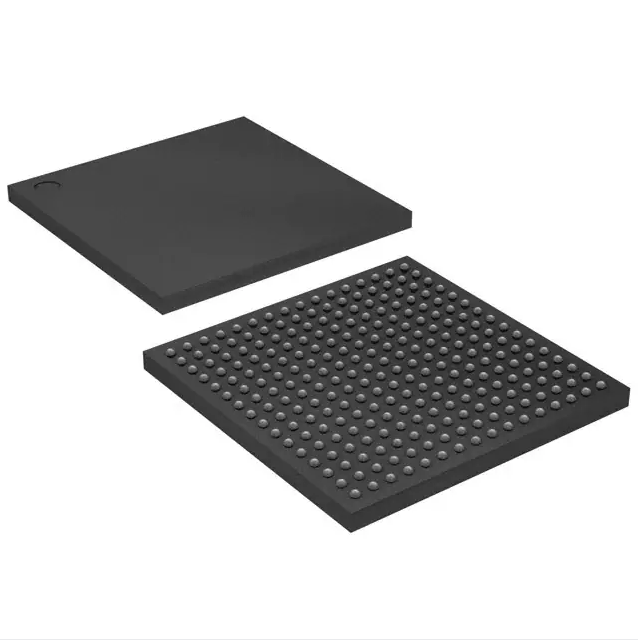
XC6SLX9 XC6SLX16-2FTG256I new original integrat...
-
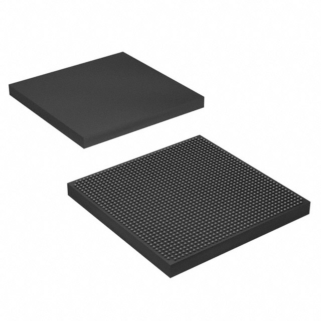
IC FPGA 520 I/O 1517FCBGA XCVU3P-2FFVC1517E ic ...
-

XCKU15P-2FFVE1517I Kintex UltraScale+FPGAs DC a...
-
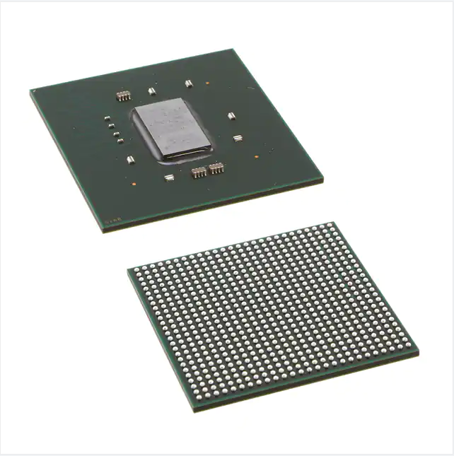
XC7K160T New and Original Electronic Components...
-

Best Price LTM4700EY#PBF One Spot Buy BOM Servi...
-
AQX XCKU040-2FFVA1156I New and original integra...