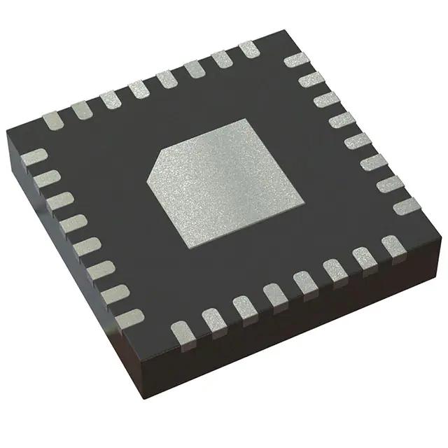
DRV5033FAQDBZR IC integrated circuit Electron
Product Attributes
| TYPE | DESCRIPTION |
| Category | Sensors, Transducers
Magnetic Sensors - Switches (Solid State) |
| Mfr | Texas Instruments |
| Series | - |
| Package | Tape & Reel (TR)
Cut Tape (CT) Digi-Reel® |
| Part Status | Active |
| Function | Omnipolar Switch |
| Technology | Hall Effect |
| Polarization | North Pole, South Pole |
| Sensing Range | 3.5mT Trip, 2mT Release |
| Test Condition | -40°C ~ 125°C |
| Voltage - Supply | 2.5V ~ 38V |
| Current - Supply (Max) | 3.5mA |
| Current - Output (Max) | 30mA |
| Output Type | Open Drain |
| Features | - |
| Operating Temperature | -40°C ~ 125°C (TA) |
| Mounting Type | Surface Mount |
| Supplier Device Package | SOT-23-3 |
| Package / Case | TO-236-3, SC-59, SOT-23-3 |
| Base Product Number | DRV5033 |
Integrated Circuit Type
Compared with electrons, photons have no static mass, weak interaction, strong anti-interference ability, and are more suitable for information transmission. Optical interconnection is expected to become the core technology to break through the power consumption wall, storage wall and communication wall. Illuminant, coupler, modulator, waveguide devices are integrated into the high density optical features such as photoelectric integrated micro system, can realize quality, volume, power consumption of high density photoelectric integration, photoelectric integration platform including III - V compound semiconductor monolithic integrated (INP) passive integration platform, silicate or glass (planar optical waveguide, PLC) platform and silicon-based platform.
InP platform is mainly used for the production of laser, modulator, detector and other active devices, low technology level, high substrate cost; Using PLC platform to produce passive components, low loss, large volume; The biggest problem with both platforms is that the materials are not compatible with silicon-based electronics. The most prominent advantage of silicon-based photonic integration is that the process is compatible with CMOS process and the production cost is low, so it is considered to be the most potential optoelectronic and even all-optical integration scheme
There are two integration methods for silicon-based photonic devices and CMOS circuits.
The advantage of the former is that the photonic devices and electronic devices can be optimized separately, but the subsequent packaging is difficult and commercial applications are limited. The latter is difficult to design and process integration of the two devices. At present, hybrid assembly based on nuclear particle integration is the best choice
Classified by application field

In terms of application fields, A chip can be divided into CLOUD data center AI chip and intelligent terminal AI chip. In terms of function, it can be divided into AI Training chip and AI Inference chip. At present, the cloud market is basically dominated by NVIDIA and Google. In 2020, the optical 800AI chip developed by Ali Dharma Institute also enters the competition of cloud reasoning. There are more end players.
AI chips are widely used in data centers (IDC), mobile terminals, intelligent security, automatic driving, smart home and so on.
The Data Center
For training and reasoning in the cloud, where most training is currently done. Video content review and personalized recommendation on mobile Internet are typical cloud reasoning applications. Nvidia Gpus are the best in training and the best in reasoning. At the same time, FPGA and ASIC continue to compete for GPU market share due to their advantages of low power consumption and low cost. At present, the cloud chips mainly include NviDIa-Tesla V100 and Nvidia-Tesla T4910MLU270
Intelligent security
The main task of intelligent security is video structuring. By adding THE AI chip in the camera terminal, real-time response can be realized and bandwidth pressure can be reduced. In addition, the reasoning function can also be integrated into the edge server product to realize the background AI reasoning for non-intelligent camera data. AI chips need to be capable of video processing and decoding, mainly considering the number of video channels that can be processed and the cost of structuring a single video channel. Representative chips include HI3559-AV100, Haisi 310 and Bitmain BM1684.