


DS90UB953TRHBRQ1 ( Electronic Components IC Chips Integrated Circuits IC ) DS90UB953TRHBRQ1
Product Attributes
| TYPE | DESCRIPTION |
SELECT |
| Category | Integrated Circuits (ICs)Interface
Serializers, Deserializers |
|
| Mfr | Texas Instruments |
|
| Series | Automotive, AEC-Q100 |
|
| Package | Tape & Reel (TR)Cut Tape (CT)
Digi-Reel® |
|
| Product Status | Active |
|
| Function | Serializer |
|
| Data Rate | 4.16Gbps |
|
| Input Type | CSI-2, MIPI |
|
| Output Type | FPD-Link III, LVDS |
|
| Number of Inputs | 1 |
|
| Number of Outputs | 1 |
|
| Voltage - Supply | 1.71V ~ 1.89V |
|
| Operating Temperature | -40°C ~ 105°C |
|
| Mounting Type | Surface Mount, Wettable Flank |
|
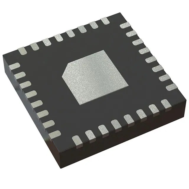
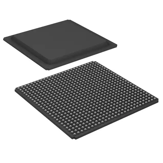
| Package / Case | 32-VFQFN Exposed Pad |
|
| Supplier Device Package | 32-VQFN (5x5) |
|
| Base Product Number | DS90UB953 |
|
| SPQ | 3000PCS |
A Serializer/Deserializer (SerDes) is a pair of functional blocks commonly used in high speed communications to compensate for limited input/output. These blocks convert data between serial data and parallel interfaces in each direction. The term "SerDes" generically refers to interfaces used in various technologies and applications. The primary use of a SerDes is to provide data transmission over a single line or a differential pair in order to minimize the number of I/O pins and interconnects.
The basic SerDes function is made up of two functional blocks: the Parallel In Serial Out (PISO) block (aka Parallel-to-Serial converter) and the Serial In Parallel Out (SIPO) block (aka Serial-to-Parallel converter). There are 4 different SerDes architectures: (1) Parallel clock SerDes, (2) Embedded clock SerDes, (3) 8b/10b SerDes, (4) Bit interleaved SerDes.
The PISO (Parallel Input, Serial Output) block typically has a parallel clock input, a set of data input lines, and input data latches. It may use an internal or external phase-locked loop (PLL) to multiply the incoming parallel clock up to the serial frequency. The simplest form of the PISO has a single shift register that receives the parallel data once per parallel clock, and shifts it out at the higher serial clock rate. Implementations may also make use of a double-buffered register to avoid metastability when transferring data between clock domains.
The SIPO (Serial Input, Parallel Output) block typically has a receive clock output, a set of data output lines and output data latches. The receive clock may have been recovered from the data by the serial clock recovery technique. However, SerDes which do not transmit a clock use reference clock to lock the PLL to the correct Tx frequency, avoiding low harmonic frequencies present in the data stream. The SIPO block then divides the incoming clock down to the parallel rate. Implementations typically have two registers connected as a double buffer. One register is used to clock in the serial stream, and the other is used to hold the data for the slower, parallel side.
Some types of SerDes include encoding/decoding blocks. The purpose of this encoding/decoding is typically to place at least statistical bounds on the rate of signal transitions to allow for easier clock recovery in the receiver, to provide framing, and to provide DC balance.
Features for the DS90UB953-Q1
- AEC-Q100 qualified for automotive applications:ISO 10605 and IEC 61000-4-2 ESD compliant
- Device temperature Grade 2: –40°C to +105°C ambient operating temperature
- Power-over-Coax (PoC) compatible transceiver
- 4.16-Gbps grade serializer supports high-speed sensors including full HD 1080p 2.3MP 60-fps and 4MP 30-fps imagers
- D-PHY v1.2 and CSI-2 v1.3 compliant system interfacePrecision multi-camera clocking and synchronization
- Up to 4 data lanes at 832 Mbps per each lane
- Supports up to four virtual channels
- Flexible programmable output clock generator
- Advanced data protection and diagnostics including CRC data protection, sensor data integrity check, I2C write protection, voltage and temperature measurement, programmable alarm, and line fault detection
- Supports Single-ended coaxial or shielded-twisted-pair (STP) cable
- Ultra-low latency bidirectional I2C and GPIO control channel enables ISP control from ECU
- Single 1.8-V power supply
- Low (0.25 W typical) power consumption
- Functional Safety-CapableCompatible with DS90UB954-Q1, DS90UB964-Q1, DS90UB962-Q1, DS90UB936-Q1, DS90UB960-Q1, DS90UB934-Q1, and DS90UB914A-Q1 deserializers
- Documentation available to aid ISO 26262 system design
- Wide temperature range: –40°C to 105°C
- Small 5-mm × 5-mm VQFN package and PoC solution size for compact camera module designs
Description for the DS90UB953-Q1
The DS90UB953-Q1 serializer is part of TI’s FPD-Link III device family designed to support high-speed raw data sensors including 2.3MP imagers at 60-fps and as well as 4MP, 30-fps cameras, satellite RADAR, LIDAR, and Time-of-Flight (ToF) sensors. The chip delivers a 4.16-Gbps forward channel and an ultra-low latency, 50-Mbps bidirectional control channel and supports power over a single coax (PoC) or STP cable. The DS90UB953-Q1 features advanced data protection and diagnostic features to support ADAS and autonomous driving. Together with a companion deserializer, the DS90UB953-Q1 delivers precise multi-camera sensor clock and sensor synchronization.
The DS90UB953-Q1 is fully AEC-Q100 qualified with a -40°C to 105°C wide temperature range.The serializer comes in a small 5-mm × 5-mm VQFN package for space-constrained sensor applications.
-
DP83848CVVXN-NOPB New and Original Ethernet IC ...
-
DP83848CVVX/NOPB Original Electronic Component ...
-
XC7K325T-1FBG676I 676-FCBGA (27×27) integr...
-

TPA2013D1RGPR Audio Amp Speaker Electronic Comp...
-
New and Original XCKU5P-2FFVB676I IC Integrated...
-
New and Original XC6VLX240T-2FFG1759I Integrate...