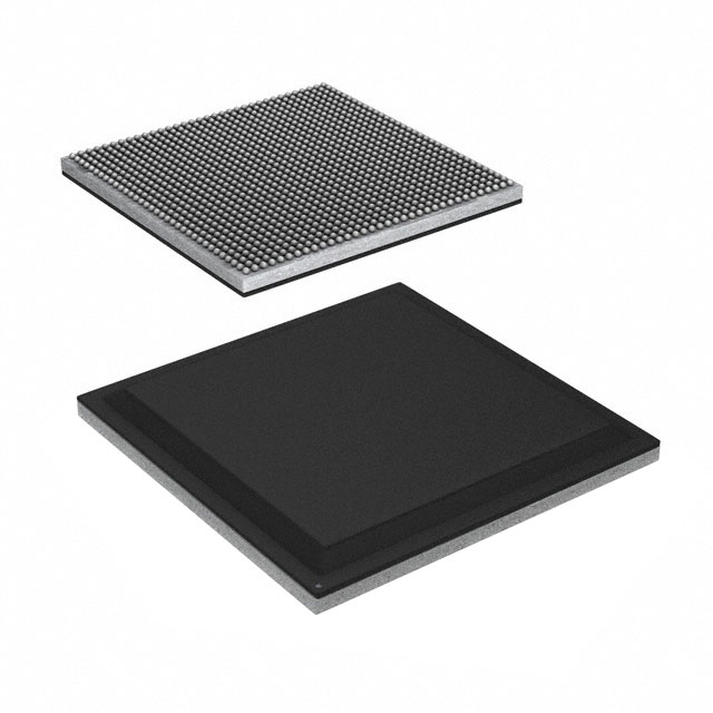
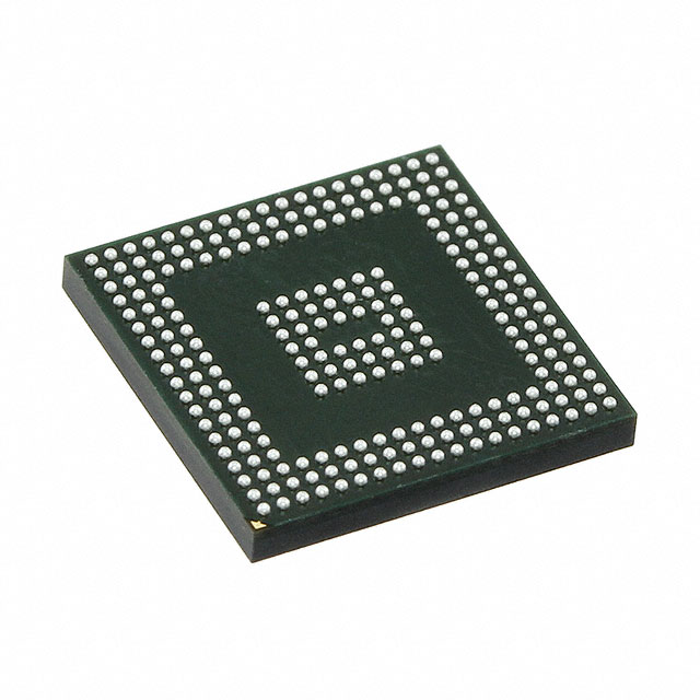
LFE5U-25F-6BG256C – Integrated Circuits, Embedded, FPGAs (Field Programmable Gate Array)
Product Attributes
| TYPE | DESCRIPTION |
| Category | Integrated Circuits (ICs) |
| Mfr | Lattice Semiconductor Corporation |
| Series | ECP5 |
| Package | Tray |
| Product Status | Active |
| DigiKey Programmable | Not Verified |
| Number of LABs/CLBs | 6000 |
| Number of Logic Elements/Cells | 24000 |
| Total RAM Bits | 1032192 |
| Number of I/O | 197 |
| Voltage - Supply | 1.045V ~ 1.155V |
| Mounting Type | Surface Mount |
| Operating Temperature | 0°C ~ 85°C (TJ) |
| Package / Case | 256-LFBGA |
| Supplier Device Package | 256-CABGA (14x14) |
| Base Product Number | LFE5U-25 |
Documents & Media
| RESOURCE TYPE | LINK |
| Datasheets | ECP5, ECP5-5G Family Datasheet |
| PCN Assembly/Origin | Mult Dev 16/Dec/2019 |
| PCN Packaging | All Dev Pkg Mark Chg 12/Nov/2018 |
Environmental & Export Classifications
| ATTRIBUTE | DESCRIPTION |
| RoHS Status | ROHS3 Compliant |
| Moisture Sensitivity Level (MSL) | 3 (168 Hours) |
| REACH Status | REACH Unaffected |
| ECCN | EAR99 |
| HTSUS | 8542.39.0001 |
FPGAs
Introduce:
Field Programmable Gate Arrays (FPGAs) have emerged as an advanced technology in digital circuit design. These programmable integrated circuits provide designers with unprecedented flexibility and customization capabilities. In this article, we delve into the world of FPGAs, exploring their structure, benefits, and applications. By understanding the capabilities and potential of FPGAs, we can understand how they have revolutionized the field of digital circuit design.
Structure and function:
FPGAs are reconfigurable digital circuits made up of programmable logic blocks, interconnects, and input/output (I/O) blocks. These blocks can be programmed using a hardware description language (HDL) such as VHDL or Verilog, allowing the designer to specify the function of the circuit. Logic blocks can be configured to perform various operations, such as arithmetic calculations or logic functions, by programming a look-up table (LUT) within the logic block. Interconnects act as paths connecting different logic blocks, facilitating communication between them. The I/O module provides an interface for external devices to interact with the FPGA. This highly adaptable structure enables designers to create complex digital circuits that can be easily modified or reprogrammed.
Advantages of FPGAs:
The main advantage of FPGAs is their flexibility. Unlike application-specific integrated circuits (ASICs), which are hardwired for specific functions, FPGAs can be reconfigured as needed. This allows designers to quickly prototype, test and modify circuits without the expense of creating a custom ASIC. FPGAs also offer shorter development cycles, reducing time-to-market for complex electronic systems. Additionally, FPGAs are highly parallel in nature, making them suitable for computationally intensive applications such as artificial intelligence, data encryption, and real-time signal processing. Additionally, FPGAs are more energy-efficient than general-purpose processors because they can be precisely tailored to the desired operation, minimizing unnecessary power consumption.
Applications in various industries:
Due to their versatility, FPGAs are used in various industries. In telecommunications, FPGAs are used in base stations and network routers to process high-speed data, enhance data security, and support software-defined networking. In automotive systems, FPGAs enable advanced driver assistance features such as collision avoidance and adaptive cruise control. They are also used in real-time image processing, diagnostics and patient monitoring in medical equipment. Additionally, FPGAs are integral to aerospace and defense applications, powering radar systems, avionics, and secure communications. Its adaptability and outstanding performance characteristics make FPGA an important part of cutting-edge technology in various fields.
Challenges and future directions:
Although FPGAs have many advantages, they also present their own set of challenges. The FPGA design process can be complex, requiring expertise and expertise in hardware description languages and FPGA architecture. Additionally, FPGAs consume more power than ASICs while performing the same task. However, ongoing research and development is addressing these challenges. New tools and methodologies are being developed to simplify FPGA design and reduce power consumption. As technology continues to advance, FPGAs are expected to become more powerful, more power-efficient, and available to a wider range of designers.
In conclusion:
Field Programmable Gate Arrays have changed the field of digital circuit design. Their flexibility, reconfigurability and versatility make them indispensable in various industries. From telecommunications to automotive and aerospace, FPGAs enable advanced functionality and superior performance. Despite the challenges, continued progress promises to overcome them and further enhance the capabilities and applications of these remarkable devices. With the growing demand for complex and custom electronic systems, FPGAs will undoubtedly play a vital role in shaping the future of digital circuit design.