


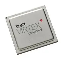
XCVU190-2FLGB2104I 100% New & Original Own Stock Integrated Circuit High-Performance Clock Buffer Family
Product Attributes
| TYPE | DESCRIPTION |
| Category | FPGAs (Field Programmable Gate Array) |
| Mfr | AMD |
| Series | Virtex® UltraScale™ |
| Package | Tray |
| Product Status | Active |
| DigiKey Programmable | Not Verified |
| Number of LABs/CLBs | 134280 |
| Number of Logic Elements/Cells | 2349900 |
| Total RAM Bits | 150937600 |
| Number of I/O | 702 |
| Voltage - Supply | 0.922V ~ 0.979V |
| Mounting Type | Surface Mount |
| Operating Temperature | -40°C ~ 100°C (TJ) |
| Package / Case | 2104-BBGA, FCBGA |
| Supplier Device Package | 2104-FCBGA (47.5x47.5) |
| Base Product Number | XCVU190 |
Description
Kintex® UltraScale FPGAs: High-performance FPGAs with a focus on price/performance, using both monolithic and next-generation stacked silicon interconnect (SSI) technology. High DSP and block RAM-to-logic ratios and next-generation transceivers, combined with low-cost packaging, enable an optimum blend of capability and cost.
Kintex UltraScale+™ FPGAs: Increased performance and on-chip UltraRAM memory to reduce BOM cost. The ideal mix of high-performance peripherals and cost-effective system implementation. Kintex UltraScale+ FPGAs have numerous power options that deliver the optimal balance between the required system performance and the smallest power envelope.
Virtex® UltraScale FPGAs: High-capacity, high-performance FPGAs enabled using both monolithic and next-generation SSI technology. Virtex UltraScale devices achieve the highest system capacity, bandwidth, and performance to address key market and application requirements through integration of various system level functions.
Virtex UltraScale+ FPGAs: The highest transceiver bandwidth, highest DSP count, and highest on-chip and in-package memory available in the UltraScale architecture. Virtex UltraScale+ FPGAs also provide numerous power options that deliver the optimal balance between the required system performance and the smallest power envelope.
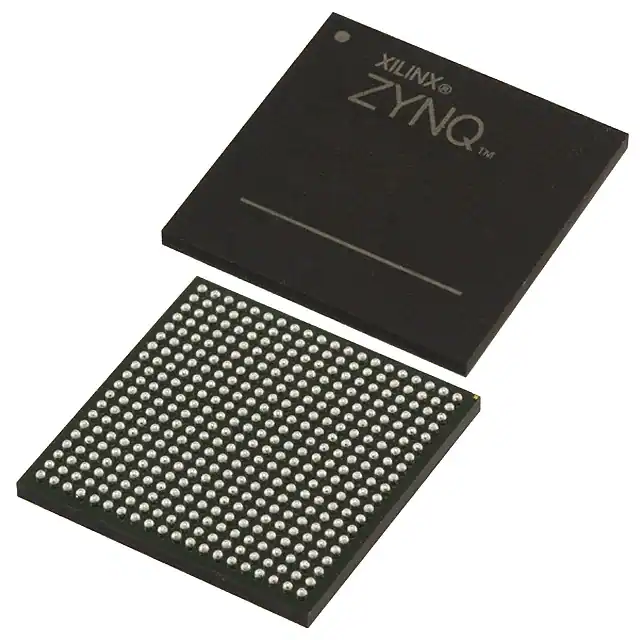
Zynq® UltraScale+ MPSoCs: Combine the ARM® v8-based Cortex®-A53 high-performance energy-efficient 64-bit application processor with the ARM Cortex-R5 real-time processor and the UltraScale architecture to create the industry's first All Programmable MPSoCs. Provide unprecedented power savings, heterogeneous processing, and programmable acceleration. Zynq® UltraScale+ RFSoCs: Combine RF data converter subsystem and forward error correction with industry-leading programmable logic and heterogeneous processing capability.Integrated RF-ADCs, RF-DACs, and soft-decision FECs (SD-FEC) provide the key subsystems for multiband, multi-mode cellular radios and cable infrastructure.
Summary of Features
-
.png)
TPS62130AQRGTRQ1 VQFN16 Components Distribution...
-
SN74LVC3G07YZPR Original And New With Competiti...
-
.png)
One Stop Service SON8 TPS7A8101QDRBRQ1 With Ori...
-
Electronic Components IC Chips Integrated Circu...
-
Xc7z010-1clg400i Xc7z010-1clg400i In Stock Orig...
-
Electronic Components IC Chips Integrated Circu...