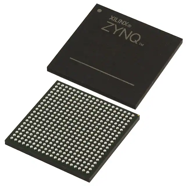
10AX066H3F34E2SG 100% New & Original Isolation Amplifier 1 Circuit Differential 8-SOP
Product Attributes
| EU RoHS | Compliant |
| ECCN (US) | 3A001.a.7.b |
| Part Status | Active |
| HTS | 8542.39.00.01 |
| Automotive | No |
| PPAP | No |
| Family Name | Arria® 10 GX |
| Process Technology | 20nm |
| User I/Os | 492 |
| Number of Registers | 1002160 |
| Operating Supply Voltage (V) | 0.9 |
| Logic Elements | 660000 |
| Number of Multipliers | 3356 (18x19) |
| Program Memory Type | SRAM |
| Embedded Memory (Kbit) | 42660 |
| Total Number of Block RAM | 2133 |
| Device Logic Units | 660000 |
| Device Number of DLLs/PLLs | 16 |
| Transceiver Channels | 24 |
| Transceiver Speed (Gbps) | 17.4 |
| Dedicated DSP | 1678 |
| PCIe | 2 |
| Programmability | Yes |
| Reprogrammability Support | Yes |
| Copy Protection | Yes |
| In-System Programmability | Yes |
| Speed Grade | 3 |
| Single-Ended I/O Standards | LVTTL|LVCMOS |
| External Memory Interface | DDR3 SDRAM|DDR4|LPDDR3|RLDRAM II|RLDRAM III|QDRII+SRAM |
| Minimum Operating Supply Voltage (V) | 0.87 |
| Maximum Operating Supply Voltage (V) | 0.93 |
| I/O Voltage (V) | 1.2|1.25|1.35|1.5|1.8|2.5|3 |
| Minimum Operating Temperature (°C) | 0 |
| Maximum Operating Temperature (°C) | 100 |
| Supplier Temperature Grade | Extended |
| Tradename | Arria |
| Mounting | Surface Mount |
| Package Height | 2.63 |
| Package Width | 35 |
| Package Length | 35 |
| PCB changed | 1152 |
| Standard Package Name | BGA |
| Supplier Package | FC-FBGA |
| Pin Count | 1152 |
| Lead Shape | Ball |
Integrated Circuit Type
Compared with electrons, photons have no static mass, weak interaction, strong anti-interference ability, and are more suitable for information transmission. Optical interconnection is expected to become the core technology to break through the power consumption wall, storage wall and communication wall. Illuminant, coupler, modulator, waveguide devices are integrated into the high density optical features such as photoelectric integrated micro system, can realize quality, volume, power consumption of high density photoelectric integration, photoelectric integration platform including III - V compound semiconductor monolithic integrated (INP) passive integration platform, silicate or glass (planar optical waveguide, PLC) platform and silicon-based platform.
InP platform is mainly used for the production of laser, modulator, detector and other active devices, low technology level, high substrate cost; Using PLC platform to produce passive components, low loss, large volume; The biggest problem with both platforms is that the materials are not compatible with silicon-based electronics. The most prominent advantage of silicon-based photonic integration is that the process is compatible with CMOS process and the production cost is low, so it is considered to be the most potential optoelectronic and even all-optical integration scheme
There are two integration methods for silicon-based photonic devices and CMOS circuits.
The advantage of the former is that the photonic devices and electronic devices can be optimized separately, but the subsequent packaging is difficult and commercial applications are limited. The latter is difficult to design and process integration of the two devices. At present, hybrid assembly based on nuclear particle integration is the best choice