


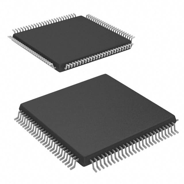
Integrated circuit IC chips one spot buy EPM240T100C5N IC CPLD 192MC 4.7NS 100TQFP
Product Attributes
| TYPE | DESCRIPTION |
| Category | Integrated Circuits (ICs) Embedded CPLDs (Complex Programmable Logic Devices) |
| Mfr | Intel |
| Series | MAX® II |
| Package | Tray |
| Standard Package | 90 |
| Product Status | Active |
| Programmable Type | In System Programmable |
| Delay Time tpd(1) Max | 4.7 ns |
| Voltage Supply – Internal | 2.5V, 3.3V |
| Number of Logic Elements/Blocks | 240 |
| Number of Macrocells | 192 |
| Number of I/O | 80 |
| Operating Temperature | 0°C ~ 85°C (TJ) |
| Mounting Type | Surface Mount |
| Package / Case | 100-TQFP |
| Supplier Device Package | 100-TQFP (14×14) |
| Base Product Number | EPM240 |
The cost has been one of the major issues facing 3D packaged chips, and Foveros will be the first time Intel has produced them in high volume thanks to its leading packaging technology. Intel, however, says that chips produced in 3D Foveros packages are extremely price competitive with standard chip designs – and in some cases may even be cheaper.
Intel has designed the Foveros chip to be as low-cost as possible and still meet the company’s stated performance goals – it is the cheapest chip in the Meteor Lake package. Intel has not yet shared the speed of the Foveros interconnect / base tile but has said that the components can run at a few GHz’ in a passive configuration (a statement that implies the existence of an active version of the intermediary layer Intel is already developing). Thus, Foveros does not require the designer to compromise on bandwidth or latency constraints.
Intel also expects the design to scale well in terms of both performance and cost, meaning it can offer specialized designs for other market segments, or variants of the high-performance version.
The cost of advanced nodes per transistor is growing exponentially as silicon chip processes approach their limits. And designing new IP modules (such as I/O interfaces) for smaller nodes does not provide much return on investment. Therefore, reusing non-critical tiles/chiplets on ‘good enough’ existing nodes can save time, cost, and development resources, not to mention simplifying the testing process.
For single chips, Intel must test different chip elements, such as memory or PCIe interfaces, in succession, which can be a time-consuming process. In contrast, chip manufacturers can also test small chips simultaneously to save time. covers also have an advantage in designing chips for specific TDP ranges, as designers can customize different small chips to suit their design needs.
Most of these points sound familiar, and they are all the same factors that led AMD down the chipset path in 2017. AMD wasn’t the first to use chipset-based designs, but it was the first major manufacturer to use this design philosophy to mass-produce modern chips, something Intel seems to have come to a bit late. However, Intel’s proposed 3D packaging technology is far more complex than AMD’s organic intermediary layer-based design, which has both advantages and disadvantages.
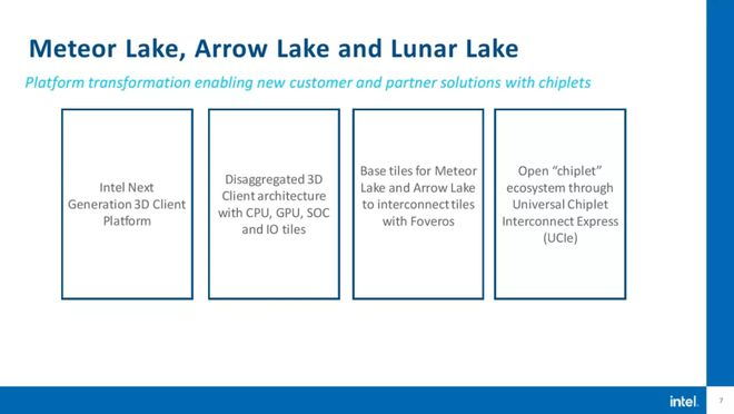
The difference will eventually be reflected in the finished chips, with Intel saying that the new 3D stacked chip Meteor Lake is expected to be available in 2023, with Arrow Lake and Lunar Lake coming in 2024.
Intel also said that the Ponte Vecchio supercomputer chip, which will have more than 100 billion transistors, is expected to be at the heart of Aurora, the world’s fastest supercomputer.
-
XCKU060-1FFVA1156I Original New With Best Price...
-
Merrill chip New & Original in stock elect...
-
Integrated Circuits IRFR3504ZTRPBF Contact Best...
-
New Original XC7A15T-L2CSG324E Inventory Spot I...
-
.png)
LVDS Serializer 2975Mbps Automotive 40-Pin WQFN...
-
Semicon Fast Delivery Electronic Components Chi...