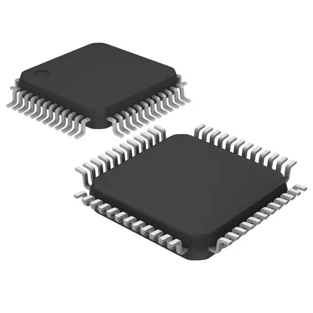
XCZU19EG-2FFVC1760E 100% New & Original DC To DC Converter & Switching Regulator Chip
Product Attributes
| Product Attribute | Attribute Value |
| Manufacturer: | Xilinx |
| Product Category: | SoC FPGA |
| Shipping Restrictions: | This product may require additional documentation to export from the United States. |
| RoHS: | Details |
| Mounting Style: | SMD/SMT |
| Package / Case: | FBGA-1760 |
| Core: | ARM Cortex A53, ARM Cortex R5, ARM Mali-400 MP2 |
| Number of Cores: | 7 Core |
| Maximum Clock Frequency: | 600 MHz, 667 MHz, 1.5 GHz |
| L1 Cache Instruction Memory: | 2 x 32 kB, 4 x 32 kB |
| L1 Cache Data Memory: | 2 x 32 kB, 4 x 32 kB |
| Program Memory Size: | - |
| Data RAM Size: | - |
| Number of Logic Elements: | 1143450 LE |
| Adaptive Logic Modules - ALMs: | 65340 ALM |
| Embedded Memory: | 34.6 Mbit |
| Operating Supply Voltage: | 850 mV |
| Minimum Operating Temperature: | 0 C |
| Maximum Operating Temperature: | + 100 C |
| Brand: | Xilinx |
| Distributed RAM: | 9.8 Mbit |
| Embedded Block RAM - EBR: | 34.6 Mbit |
| Moisture Sensitive: | Yes |
| Number of Logic Array Blocks - LABs: | 65340 LAB |
| Number of Transceivers: | 72 Transceiver |
| Product Type: | SoC FPGA |
| Series: | XCZU19EG |
| Factory Pack Quantity: | 1 |
| Subcategory: | SOC - Systems on a Chip |
| Tradename: | Zynq UltraScale+ |
Integrated Circuit Type
Compared with electrons, photons have no static mass, weak interaction, strong anti-interference ability, and are more suitable for information transmission. Optical interconnection is expected to become the core technology to break through the power consumption wall, storage wall and communication wall. Illuminant, coupler, modulator, waveguide devices are integrated into the high density optical features such as photoelectric integrated micro system, can realize quality, volume, power consumption of high density photoelectric integration, photoelectric integration platform including III - V compound semiconductor monolithic integrated (INP) passive integration platform, silicate or glass (planar optical waveguide, PLC) platform and silicon-based platform.
InP platform is mainly used for the production of laser, modulator, detector and other active devices, low technology level, high substrate cost; Using PLC platform to produce passive components, low loss, large volume; The biggest problem with both platforms is that the materials are not compatible with silicon-based electronics. The most prominent advantage of silicon-based photonic integration is that the process is compatible with CMOS process and the production cost is low, so it is considered to be the most potential optoelectronic and even all-optical integration scheme
There are two integration methods for silicon-based photonic devices and CMOS circuits.
The advantage of the former is that the photonic devices and electronic devices can be optimized separately, but the subsequent packaging is difficult and commercial applications are limited. The latter is difficult to design and process integration of the two devices. At present, hybrid assembly based on nuclear particle integration is the best choice