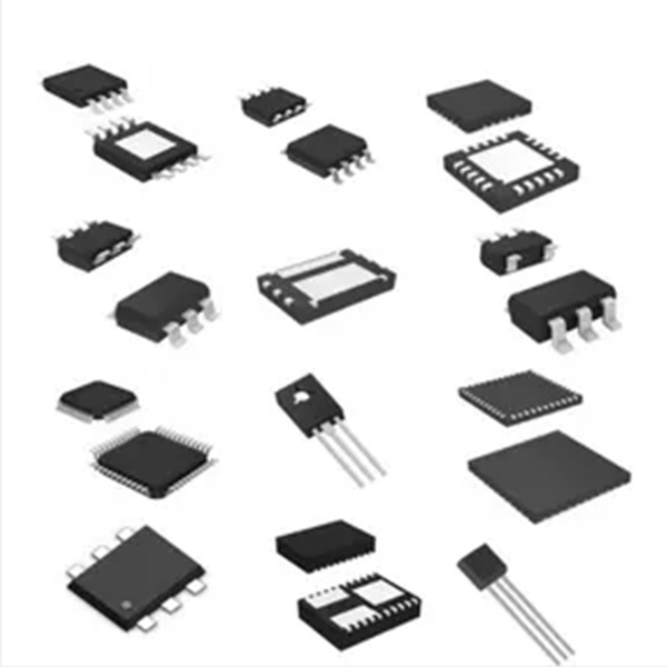
Electronic Components Circuit Bom List Mcu TLC7733IDR LMR33630BQRNXRQ1 LM431CIM3/NOPB TMS320F28033PAGT IC Chip

Product Attributes
| TYPE | DESCRIPTION |
| Category | Integrated Circuits (ICs) |
| Mfr | Texas Instruments |
| Series | Automotive, AEC-Q100 |
| Package | Tape & Reel (TR) |
| SPQ | 3000T&R |
| Product Status | Active |
| Function | Step-Down |
| Output Configuration | Positive |
| Topology | Buck |
| Output Type | Adjustable |
| Number of Outputs | 1 |
| Voltage - Input (Min) | 3.8V |
| Voltage - Input (Max) | 36V |
| Voltage - Output (Min/Fixed) | 1V |
| Voltage - Output (Max) | 24V |
| Current - Output | 3A |
| Frequency - Switching | 1.4MHz |
| Synchronous Rectifier | Yes |
| Operating Temperature | -40°C ~ 125°C (TJ) |
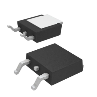
| Mounting Type | Surface Mount, Wettable Flank |
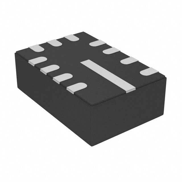
| Package / Case | 12-VFQFN |
| Supplier Device Package | 12-VQFN-HR (3x2) |
| Base Product Number | LMR33630 |
1.Design of the chip.
The first step in design, setting targets
The most important step in IC design is a specification. This is like deciding how many rooms and bathrooms you want, what building codes you need to comply with, and then proceeding with the design after you have determined all the functions so that you don't have to spend extra time on subsequent modifications; IC design needs to go through a similar process to ensure that the resulting chip will be error-free.
The first step in the specification is to determine the purpose of the IC, what the performance is, and to set the general direction. The next step is to see what protocols need to be met, such as IEEE 802.11 for a wireless card, otherwise the chip will not be compatible with other products on the market, making it impossible to connect to other devices. The final step is to establish how the IC will work, assigning different functions to different units and establishing how the different units will be connected to each other, thus completing the specification.
After designing the specifications, it is then time to design the details of the chip. This step is like the initial drawing of a building, where the overall outline is sketched out to facilitate subsequent drawings. In the case of IC chips, this is done by using a hardware description language (HDL) to describe the circuit. HDLs such as Verilog and VHDL are commonly used to easily express the functions of an IC through programming code. Then the program is checked for correctness and modified until it meets the desired function.
Layers of photomasks, stacking up a chip
First of all, it is now known that an IC produces multiple photomasks, which have different layers, each with its task. The diagram below shows a simple example of a photomask, using CMOS, the most basic component in an integrated circuit, as an example. CMOS is a combination of NMOS and PMOS, forming CMOS.
Each of the steps described here has its special knowledge and can be taught as a separate course. For example, writing a hardware description language requires not only familiarity with the programming language, but also an understanding of how logic circuits work, how to convert the required algorithms into programs, and how synthesis software converts programs into logic gates.
2.What is a wafer?
In semiconductor news, there are always references to fabs in terms of size, such as 8" or 12" fabs, but what exactly is a wafer? What part of 8" does it refer to? And what are the difficulties of manufacturing large wafers? The following is a step-by-step guide to what a wafer is, the most important foundation of a semiconductor.
Wafers are the basis for manufacturing all kinds of computer chips. We can compare chip manufacturing to building a house with Lego blocks, stacking them layer after layer to create the desired shape (i.e. various chips). However, without a good foundation, the resulting house will be crooked and not to your liking, so to make a perfect house, a smooth substrate is needed. In the case of chip manufacturing, this substrate is the wafer that will be described next.
Among solid materials, there is a special crystal structure - the monocrystalline. It has the property that atoms are arranged one after another close to each other, creating a flat surface of atoms. Monocrystalline wafers can therefore be used to meet these requirements. However, there are two main steps to produce such a material, namely purification and crystal pulling, after which the material can be completed.