


SN74CB3Q3245RGYR 100% New & Original DC To DC Converter & Switching Regulator Chip
Product Attributes
| TYPE | ILLUSTRATE |
| category | Signal switcher, multiplexer, decoder |
| manufacturer | Texas Instruments |
| series | 74CB |
| wrap | Tape and rolling packages (TR)
Insulating tape package (CT) Digi-Reel® |
| Product status | Active |
| type | Bus switch |
| circuit | 8 x 1:1 |
| Independent circuit | 1 |
| Current - Output high, low | - |
| Voltage supply source | Single power supply |
| Voltage - Power supply | 2.3V ~ 3.6V |
| Operating temperature | -40°C ~ 85°C |
| Installation type | Surface adhesive type |
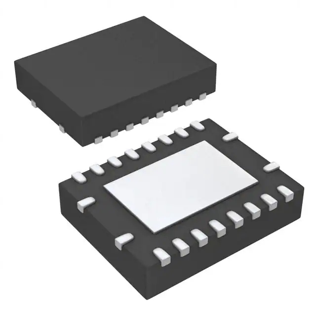
| Package/Housing | 20-VFQFN exposed pad |
| Vendor component encapsulation | 20-VQFN (3.5x4.5) |
| Product master number | 74CB3Q3245 |
Product Introduction
The SN74CB3Q3245 is a high-bandwidth FET bus switch utilizing a charge pump to elevate the gate voltage of the pass transistor, providing a low and flat ON-state resistance (ron). The low and flat ON-state resistance allows for minimal propagation delay and supports rail-to-rail switching on the data input/output (I/O) ports. The device also features low data I/O capacitance to minimize capacitive loading and signal distortion on the data bus. Specifically designed to support high-bandwidth applications, the SN74CB3Q3245 provides an optimized interface solution ideally suited for broadband communications, networking, and data-intensive computing systems.
The SN74CB3Q3245 is organized as an 8-bit bus switch with a single output-enable (OE\) input. When OE\ is low, the bus switch is ON and the A port is connected to the B port, allowing bidirectional data flow between ports. When OE\ is high, the bus switch is OFF and a high-impedance state exists between the A and B ports.
This device is fully specified for partial-power-down applications using Ioff. The Ioff circuitry prevents damaging current backflow through the device when it is powered down. The device has isolation during power off.
To ensure the high-impedance state during power up or power down, OE\ should be tied to VCC through a pullup resistor; the minimum value of the resistor is determined by the current-sinking capability of the driver.
Product Features
- High-Bandwidth Data Path (Up to 500 MHz↑)
- Equivalent to IDTQS3VH384 Device
- 5-V Tolerant I/Os with Device Powered-Up or Powered-Down
- Low and Flat ON-State Resistance (ron) Characteristics Over Operating Range (ron = 4ΩTypical)
- Rail-to-Rail Switching on Data I/O PortsBidirectional Data Flow, With Near-Zero Propagation DelayLow Input/Output Capacitance Minimizes Loading and Signal Distortion (Cio(OFF) = 3.5 pF Typical)
- 0- to 5-V Switching With 3.3-V VCC
- 0- to 3.3-V Switching With 2.5-V VCC
- Fast Switching Frequency (fOE\ = 20 MHz Max)
- Data and Control Inputs Provide Undershoot Clamp Diodes
- Low Power Consumption (ICC = 1 mA Typical)
- VCC Operating Range From 2.3 V to 3.6 V
- Data I/Os Support 0 to 5-V Signaling Levels (0.8-V, 1.2-V, 1.5-V, 1.8-V, 2.5-V, 3.3-V, 5-V)
- Control Inputs Can be Driven by TTL or 5-V/3.3-V CMOS Outputs
- Ioff Supports Partial-Power-Down Mode Operation
- Latch-Up Performance Exceeds 100 mA Per JESD 78, Class II
- ESD Performance Tested Per JESD 22Supports Both Digital and Analog Applications: PCI Interface, Differential Signal Interface, Memory Interleaving, Bus Isolation, Low-Distortion Signal Gating
- 2000-V Human-Body Model (A114-B, Class II)
- 1000-V Charged-Device Model (C101)
Product Benefits
- thermal management and overvoltage protection
Thermal management is another major challenge for battery charger designers. Every charger chip experiences a voltage drop during the charging process due to heat dissipation. To avoid battery damage or system shutdown, most chargers incorporate some form of control mechanism to manage heat build-up. Newer devices use more sophisticated feedback techniques to continuously monitor die temperature and adjust the charge current dynamically or by calculation at a rate proportional to the change in ambient temperature. This built-in intelligence allows the current charger chip to gradually reduce the charging current until thermal equilibrium is reached and the die temperature stops rising. This technology allows the charger to continuously charge the battery at the maximum possible current without causing the system to shut down, thus reducing battery charging time. Most newer devices today will also typically add an overvoltage protection mechanism.
The charger BQ25616JRTWRprovides various safety features for battery charging and system operations, including battery negative temperature coefficient thermistor monitoring, charging safety timer and overvoltage and over-current protections. Thermal regulation reduces charge current when the junction temperature exceeds 110°C. The STAT output reports the charging status and any fault conditions.
Application Scenarios
The battery charger chip belongs to a kind of power management chip, the application range is very wide. The development of power management chips is important for improving the performance of the whole machine, the choice of power management chips is directly related to the needs of the system, while the development of digital power management chips still needs to cross the cost barrier.
The BQ25616/616J is a highly integrated 3-A switch-mode battery charge management and system power path management device for single cell Li-Ion and Li-polymer batteries. The solution is highly integrated with input reverse-blocking FET (RBFET, Q1), high-side switching FET (HSFET, Q2), low-side switching FET (LSFET, Q3), and battery FET (BATFET, Q4) between system and battery. The low impedance power path optimizes switch-mode operation efficiency, reduces battery charging time and extends battery run time during discharging phase.
The BQ25616/616J is a highly integrated 3-A switch-mode battery charge management and system Power Path management device for Li-ion and Li-polymer batteries. It features fast charging with high input voltage support for a wide range of applications including speakers, industrial, and medical portable devices. Its low impedance power path optimizes switch-mode operation efficiency, reduces battery charging time, and extends battery run time during discharging phase. Its input voltage and current regulation deliver maximum charging power to the battery.
The solution is highly integrated with input reverse-blocking FET (RBFET, Q1), high-side switching FET (HSFET, Q2), low-side switching FET (LSFET, Q3), and battery FET (BATFET, Q4) between system and battery. It also integrates the bootstrap diode for the high-side gate drive for simplified system design. The hardware setting and status report provides easy configuration to set up the charging solution.
-
Microcontroller original new esp8266 XC7A200T-2...
-
ONEHONG New and original Integrated circuit hot...
-
New Original XC7K160T-1FBG676I Inventory Spot I...
-
IRF100S201 Advantage Supply Stock New Original ...
-

XCZU3EG-1SFVC784I Integrated Circuits Brand New...
-
IRF9540NSTRLPBF new and original Integrated cir...