


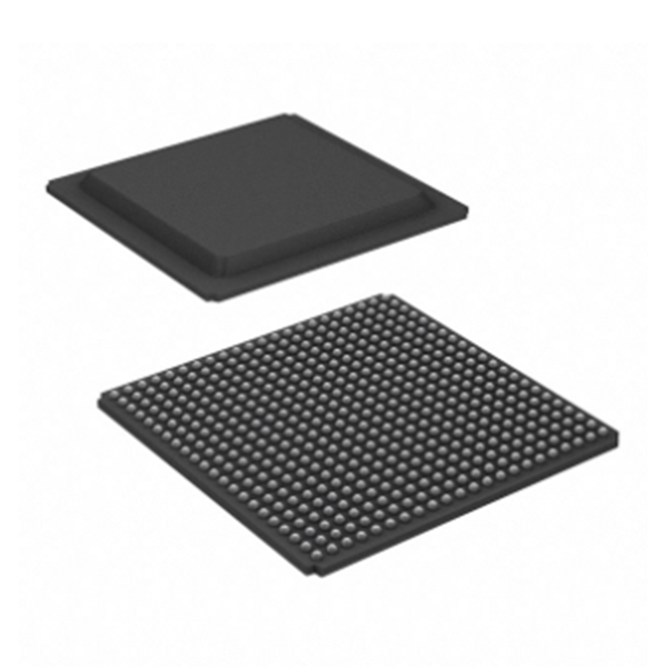
XCKU060-2FFVA1156I 100% New & Original DC To DC Converter & Switching Regulator Chip

Product Attributes
| TYPE | ILLUSTRATE |
| category | Field Programmable Gate Arrays (FPGAs) |
| manufacturer | AMD |
| series | Kintex® UltraScale™ |
| wrap | bulk |
| Product status | Active |
| DigiKey is programmable | Not verified |
| LAB/CLB number | 41460 |
| Number of logic elements/units | 725550 |
| Total number of RAM bits | 38912000 |
| Number of I/Os | 520 |
| Voltage - Power supply | 0.922V ~ 0.979V |
| Installation type | Surface adhesive type |
| Operating temperature | -40°C ~ 100°C (TJ) |
| Package/Housing | 1156-BBGA、FCBGA |
| Vendor component encapsulation | 1156-FCBGA (35x35) |
| Product master number | XCKU060 |
Integrated Circuit Type
Compared with electrons, photons have no static mass, weak interaction, strong anti-interference ability, and are more suitable for information transmission. Optical interconnection is expected to become the core technology to break through the power consumption wall, storage wall and communication wall. Illuminant, coupler, modulator, waveguide devices are integrated into the high density optical features such as photoelectric integrated micro system, can realize quality, volume, power consumption of high density photoelectric integration, photoelectric integration platform including III - V compound semiconductor monolithic integrated (INP) passive integration platform, silicate or glass (planar optical waveguide, PLC) platform and silicon-based platform.
InP platform is mainly used for the production of laser, modulator, detector and other active devices, low technology level, high substrate cost; Using PLC platform to produce passive components, low loss, large volume; The biggest problem with both platforms is that the materials are not compatible with silicon-based electronics. The most prominent advantage of silicon-based photonic integration is that the process is compatible with CMOS process and the production cost is low, so it is considered to be the most potential optoelectronic and even all-optical integration scheme
There are two integration methods for silicon-based photonic devices and CMOS circuits.
The advantage of the former is that the photonic devices and electronic devices can be optimized separately, but the subsequent packaging is difficult and commercial applications are limited. The latter is difficult to design and process integration of the two devices. At present, hybrid assembly based on nuclear particle integration is the best choice
-
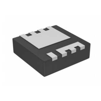
BSZ060NE2LS IC Chip New Original Integrated Cir...
-

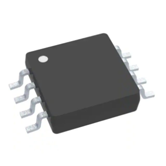
IRF7103TRPBF New And Original Integrated Circui...
-
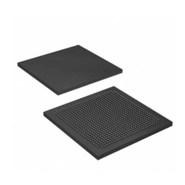
Encapsulation BGA484 embedded FPGA chip XC6SLX1...
-

New Original Electronic Component XC7Z020-1CLG4...
-
OPA1662AIDGKRQ1 New And Original Integrated Cir...
-
Original Electronic Component 5M570ZT144C5N EP2...