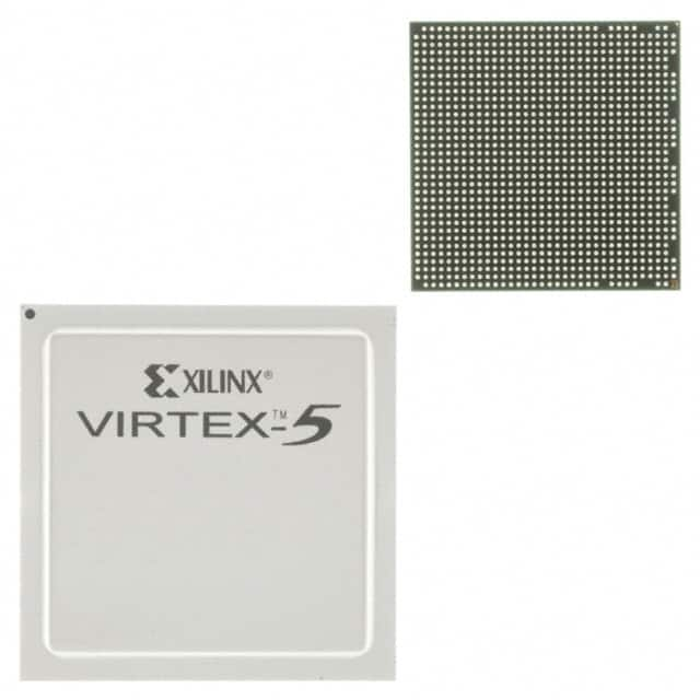
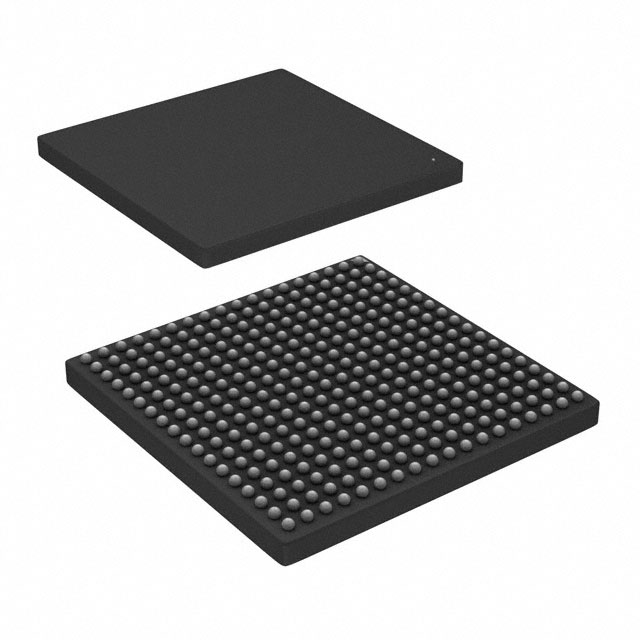
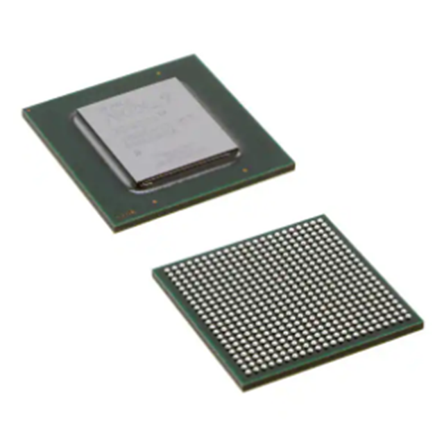
10AX115H2F34E2SG FPGA Arria® 10 GX Family 1150000 Cells 20nm Technology 0.9V 1152-Pin FC-FBGA
Product Technical Specifications
|
EU RoHS |
Compliant |
|
ECCN (US) |
3A991 |
|
Part Status |
Active |
|
HTS |
8542.39.00.01 |
|
SVHC |
Yes |
|
SVHC Exceeds Threshold |
Yes |
|
Automotive |
No |
|
PPAP |
No |
|
Family Name |
Arria® 10 GX |
|
Process Technology |
20nm |
|
User I/Os |
504 |
|
Number of Registers |
1708800 |
|
Operating Supply Voltage (V) |
0.9 |
|
Logic Elements |
1150000 |
|
Number of Multipliers |
3036 (18x19) |
|
Program Memory Type |
SRAM |
|
Embedded Memory (Kbit) |
54260 |
|
Total Number of Block RAM |
2713 |
|
EMACs |
3 |
|
Device Logic Units |
1150000 |
|
Device Number of DLLs/PLLs |
32 |
|
Transceiver Channels |
96 |
|
Transceiver Speed (Gbps) |
17.4 |
|
Dedicated DSP |
1518 |
|
PCIe |
4 |
|
Programmability |
Yes |
|
Reprogrammability Support |
Yes |
|
Copy Protection |
Yes |
|
In-System Programmability |
Yes |
|
Speed Grade |
2 |
|
Single-Ended I/O Standards |
LVTTL|LVCMOS |
|
External Memory Interface |
DDR3 SDRAM|DDR4|LPDDR3|RLDRAM II|RLDRAM III|QDRII+SRAM |
|
Minimum Operating Supply Voltage (V) |
0.87 |
|
Maximum Operating Supply Voltage (V) |
0.93 |
|
I/O Voltage (V) |
1.2|1.25|1.35|1.5|1.8|2.5|3 |
|
Minimum Operating Temperature (°C) |
0 |
|
Maximum Operating Temperature (°C) |
100 |
|
Supplier Temperature Grade |
Extended |
|
Tradename |
Arria |
|
Mounting |
Surface Mount |
|
Package Height |
2.95 |
|
Package Width |
35 |
|
Package Length |
35 |
|
PCB changed |
1152 |
|
Standard Package Name |
BGA |
|
Supplier Package |
FC-FBGA |
|
Pin Count |
1152 |
|
Lead Shape |
Ball |
The difference and relation between FPGA and CPLD
1. FPGA definition and characteristics
FPGA adopts a new concept named Logic Cell Array (LCA) and Configurable Logic Block (CLB) and Input Output (IOB) Block and Interconnect. The configurable logic module is the basic unit to realize the user function, which is usually arranged into an array and spread the whole chip. The input-output module IOB completes the interface between the logic on the chip and the external package pin, and is usually arranged around the chip array. Internal wiring consists of various lengths of wire segments and some programmable connection switches, which connect various programmable logic blocks or I/O blocks to form a circuit with a specific function.
The basic features of FPGA are:
- Using FPGA to design ASIC circuit, users do not need to project production, can get a suitable chip;
- The FPGA can be used as pilot sample of other fully customized or semi-customized ASIC circuits;
- There are abundant triggers and I/O pins in FPGA;
- FPGA is one of the devices with the shortest design cycle, the lowest development cost and the lowest risk in ASIC circuit.
- FPGA adopts high-speed CHMOS process, low power consumption, and can be compatible with CMOS and TTL levels.
2, CPLD definition and characteristics
CPLD is mainly composed of programmable Logic Macro Cell (LMC) around the center of the programmable interconnection matrix unit, in which the LMC logic structure is more complex, and has a complex I/O unit interconnection structure, can be generated by the user according to the needs of the specific circuit structure, to complete certain functions. Because the logic blocks are interconnected with fixed length metal wires in CPLD, the designed logic circuit has time predictability and avoids the disadvantage of incomplete prediction of the timing of segmented interconnect structure. By the 1990s,CPLD developed more rapidly, not only with electrical erasure characteristics, but also with advanced features such as edge scanning and online programming.
The characteristics of CPLD programming are as follows:
- Logical and memory resources are abundant (Cypress De1ta 39K200 has more than 480 Kb of RAM);
- Flexible timing model with redundant routing resources;
- Flexible to change the pin output;
- Can be installed on the system and reprogrammed;
- Large number of I/O units;
3. Differences and connections between FPGA and CPLD
CPLD is the abbreviation of complex programmable logic device,FPGA is the abbreviation of field programmable gate array, the function of the two is basically the same, but the implementation principle is slightly different, so we can sometimes ignore the difference between the two, collectively referred to as programmable logic device or CPLD/FPGA. There are several companies producing CPLD/ FPGas, the largest three being ALTERA,XILINX, and LAT-TICE. CPLD decomposition combinatorial logic function is very strong, a macro unit can decompose a dozen or even more than 20-30 combinatorial logic input. However, a LUT of FPGA can only handle the combinational logic of 4 inputs, so CPLD is suitable for designing complex combinational logic such as decoding. However, the manufacturing process of FPGA determines that the number of LUTs and triggers contained in the FPGA chip is very large, often thousands of thousands,CPLD can generally only achieve 512 logical units, and if the chip price is divided by the number of logical units, the average logical unit cost of FPGA is much lower than that of CPLD. So if a large number of triggers are used in the design, such as designing a complex timing logic, then using an FPGA is a good choice.
Although both FPGA and CPLD are programmable ASIC devices and have many common characteristics, due to the differences in the structure of CPLD and FPGA, they have their own characteristics:
- CPLD is more suitable for completing various algorithms and combinatorial logic, and FPGA is more suitable for completing sequential logic. In other words,FPGA is more suitable for flip-flop rich structure, while CPLD is more suitable for flip-flop limited and product term rich structure.
- The continuous routing structure of CPLD determines that its timing delay is uniform and predictable, while the segmented routing structure of FPGA determines that its delay is unpredictable.
- FPGA has more flexibility than CPLD in programming.
- CPLD is programmed by modifying the logic function of a fixed internal circuit, while FPGA is programmed by changing the wiring of the internal connection.
- Fpgas can be programmed under logic gates, while CPLDS are programmed under logic blocks.
- FPGA is more integrated than CPLD and has more complex wiring structure and logic implementation.
In general, the power consumption of CPLD is larger than that of FPGA, and the higher the integration degree, the more obvious.