


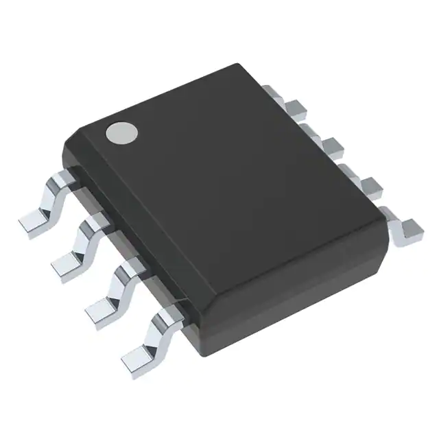
LMV358IDR Support BOM New&Original IC Integrated Circuit Components Chips Electronics Good price
Product Attributes
| TYPE | DESCRIPTION |
| Category | Integrated Circuits (ICs)
Linear - Amplifiers - Instrumentation, OP Amps, Buffer Amps |
| Mfr | Texas Instruments |
| Series | - |
| Package | Tape & Reel (TR)
Cut Tape (CT) Digi-Reel® |
| SPQ | 75Tube |
| Product Status | Active |
| Amplifier Type | General Purpose |
| Number of Circuits | 2 |
| Output Type | Rail-to-Rail |
| Slew Rate | 1V/µs |
| Gain Bandwidth Product | 1 MHz |
| Current - Input Bias | 15 nA |
| Voltage - Input Offset | 1.7 mV |
| Current - Supply | 210µA (x2 Channels) |
| Current - Output / Channel | 40 mA |
| Voltage - Supply Span (Min) | 2.7 V |
| Voltage - Supply Span (Max) | 5.5 V |
| Operating Temperature | -40°C ~ 125°C (TA) |
| Mounting Type | Surface Mount |
| Package / Case | 8-SOIC (0.154", 3.90mm Width) |
| Supplier Device Package | 8-SOIC |
| Base Product Number | LMV358 |
Technical specification
(1) Common-mode input resistance
This parameter represents the ratio of the input common-mode voltage range to the variation of the bias current within that range when the op-amp is operating in the linear region.
(2) DC common-mode rejection
This parameter is used to measure the rejection capability of an operational amplifier for the same DC signal acting on both inputs.
(3) AC common-mode rejection
CMRAC is used to measure the rejection capability of an operational amplifier for the same AC signal acting on both inputs and is a function of the differential open-loop gain divided by the common-mode open-loop gain.
(4) Gain Bandwidth Product
The gain-bandwidth product is a constant defined as the region of the open-loop gain roll-off at -20dB/decade octave in the characteristic curve with frequency.
(5) Input bias current
This parameter refers to the average current flowing into the input when the op-amp is operating in the linear region. [4]
(6) Bias current temperature drift
This parameter represents the amount of variation in the input bias current when the temperature changes. the tab is usually expressed in pA/°C.
(7) Input detuning current
This parameter is the difference between the currents flowing into the two inputs.
(8) Temperature drift of input out-of-phase current (TCIOS)
This parameter represents the amount of variation in the input detuning current due to changes in temperature. tCIOS is usually expressed in units of pA/°C.
(9) Differential mode input resistance
This parameter represents the ratio of the amount of change in input voltage to the corresponding amount of change in input current, where a change in voltage results in a change in current. When measured at one input, the other input is connected to a fixed common-mode voltage.
(10) Output impedance
This parameter is the internal equivalent small-signal impedance at the output when the operational amplifier is operating in the linear region.
(11) Output voltage swing
This parameter is the peak-to-peak value of the maximum voltage swing that can be achieved without clamping the output signal, VO is generally defined at a specific load resistance and supply voltage.
(12) Power consumption
Indicates the static power consumed by the device at a given supply voltage, Pd is usually defined at no load.
(13) Power Supply Rejection Ratio
This parameter is used to measure the ability of an operational amplifier to keep its output unchanged when the supply voltage varies. PSRR is usually expressed as the amount of change in the input detuning voltage due to a change in supply voltage.
(14) Conversion rate
This parameter is the maximum value of the ratio of the amount of change in output voltage to the time required for this change to occur. sR is usually expressed in V/µ's, and is sometimes expressed as a positive change and a negative change respectively.
(15) Supply current
This parameter is the quiescent current consumed by the device at the specified supply voltage, these parameters are usually defined in the no-load case.
(16) Unit gain bandwidth
This parameter refers to the maximum operating frequency of the op-amp when the open-loop gain is greater than 1.
(17) Input detuning voltage
This parameter indicates the voltage difference that needs to be applied at the input to make the output voltage zero.
(18) Input detuning voltage temperature drift (TCVOS)
This parameter refers to the change in the input detuning voltage caused by a change in temperature, usually expressed in units of uV/°C.
(19) Input capacitance
CIN indicates the equivalent capacitance of any one input when the op-amp is operating in the linear region (the other input is grounded).
(20) Input voltage range
This parameter refers to the range of input voltages allowed when the op-amp is operating normally (and the desired results can be obtained), VIN is usually defined at the specified supply voltage.
(21) Input voltage noise density (eN)
For operational amplifiers, the input voltage noise can be thought of as a series noise voltage source connected to either input. eN is usually expressed in nV / root Hz and is defined at the specified frequency.
(22) Input current noise density (iN)
For operational amplifiers, the input current noise can be thought of as two noise current sources connected to each input and the common terminal, usually expressed in units of pA/root Hz, defined at the specified frequency.
(23) Ideal operational amplifier parameters
Differential-mode amplification, differential-mode input resistance, common-mode rejection ratio, and upper limit frequency are infinite; the input detuned voltage and its temperature drift, the input detuned current and its temperature drift, and the noise are all zero.
-
Semiconductors Electronic Components TPS7A5201Q...
-
Brand New Electronic Component XC7A25T-2CSG325C...
-
components IC chip integrated chips electronics...
-
Brand new genuine original IC stock Electronic ...
-

XC7A15T-2CSG325I Artix-7 Field Programmable Gat...
-
electronic components Support BOM Quotation XC3...