


New and Original Sharp LCD Display LM61P101 LM64P101 LQ10D367 LQ10D368 ONE SPOT BUY
Product Attributes
| TYPE | DESCRIPTION |
| Category | Integrated Circuits (ICs) |
| Mfr | Texas Instruments |
| Series | Automotive, AEC-Q100 |
| Package | Tube |
| SPQ | 2500T&R |
| Product Status | Active |
| Output Type | Transistor Driver |
| Function | Step-Up, Step-Down |
| Output Configuration | Positive |
| Topology | Buck, Boost |
| Number of Outputs | 1 |
| Output Phases | 1 |
| Voltage - Supply (Vcc/Vdd) | 3V ~ 42V |
| Frequency - Switching | Up to 500kHz |
| Duty Cycle (Max) | 75% |
| Synchronous Rectifier | No |
| Clock Sync | Yes |
| Serial Interfaces | - |
| Control Features | Enable, Frequency Control, Ramp, Soft Start |
| Operating Temperature | -40°C ~ 125°C (TJ) |
| Mounting Type | Surface Mount |
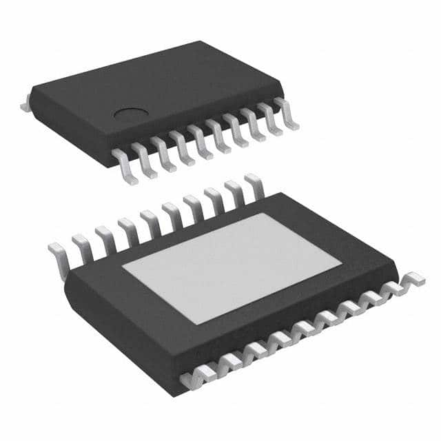
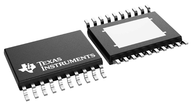
| Package / Case | 20-PowerTSSOP (0.173", 4.40mm Width) |
| Supplier Device Package | 20-HTSSOP |
| Base Product Number | LM25118 |
1.How to make a single crystal wafer
The first step is metallurgical purification, which involves adding carbon and converting silicon oxide to silicon of 98% or more purity using redox. Most metals, such as iron or copper, are refined in this way to obtain sufficiently pure metal. However, 98% is still not sufficient for chip manufacturing and further improvements are needed. Therefore, the Siemens process will be used for further purification to obtain the high-purity polysilicon required for the semiconductor process.
The next step is to pull the crystals. First, the high-purity polysilicon obtained earlier is melted down to form liquid silicon. Afterward, a single crystal of seed silicon is brought into contact with the liquid surface and slowly pulled upwards while rotating. The reason for the need for a single crystal seed is that, just like a person lining up, the silicon atoms need to be lined up so that those who come after them know how to line up correctly. Finally, when the silicon atoms have left the liquid surface and solidified, the neatly arranged single crystal silicon column is complete.
But what do the 8" and 12" represent? He is referring to the diameter of the pillar we produce, the part that looks like a pencil shaft after the surface has been treated and sliced into thin wafers. What is the difficulty in making large wafers? As mentioned earlier, the process of making wafers is like making marshmallows, spinning and shaping them as you go. Anyone who has made marshmallows before will know that it is very difficult to make large, solid marshmallows, and the same goes for the wafer pulling process, where the speed of rotation and temperature control affect the quality of the wafer. As a result, the larger the size, the higher the speed and temperature requirements, making it even more difficult to produce a high-quality 12" wafer than an 8" wafer.
To produce a wafer, a diamond cutter is then used to cut the wafer horizontally into wafers, which are then polished to form the wafers required for chip manufacturing. The next step is the stacking of houses or chip manufacturing. How do you make a chip?
2.Having been introduced to what silicon wafers are, it is also clear that manufacturing IC chips are like building a house with Lego blocks, by stacking them layer upon layer to create the shape you want. However, there are quite a few steps to building a house, and the same goes for IC manufacturing. What are the steps involved in manufacturing an IC? The following section describes the process of IC chip manufacturing.
Before we begin, we need to understand what an IC chip is - IC, or Integrated Circuit, as it is called, is a stack of designed circuits that are put together in a stacked fashion. By doing this, we can reduce the amount of area required to connect the circuits. The diagram below shows a 3D diagram of an IC circuit, which can be seen to be structured like the beams and columns of a house, stacked one on top of the other, which is why IC manufacturing is likened to building a house.
From the 3D section of the IC chip shown above, the dark blue part at the bottom is the wafer introduced in the previous section. The red and earth-colored parts are where the IC is made.
First of all, the red part can be compared to the ground floor hall of a tall building. The ground floor lobby is the gateway to the building, where access is gained, and is often more functional in terms of controlling traffic. It is therefore more complex to build than other floors and requires more steps. In the IC circuit, this hall is the logic gate layer, which is the most important part of the entire IC, combining various logic gates to create a fully functional IC chip.
The yellow part is like a normal floor. Compared to the ground floor, it is not too complex and does not change much from floor to floor. The purpose of this floor is to connect the logic gates in the red section together. The reason for the need for so many layers is that there are too many circuits to be linked together and if a single layer cannot accommodate all the circuits, several layers have to be stacked to achieve this goal. In this case, the different layers are connected up and down to meet the wiring requirements.

.png)