


-
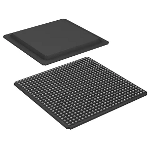
XC7Z035-2FFG676I – Integrated Circuits (ICs), Embedded, System On Chip (SoC)
The Zynq-7000 family offers the flexibility and scalability of an FPGA, while providing performance, power, and ease of use typically associated with ASIC and ASSPs. The range of devices in the Zynq-7000 family allows designers to target cost-sensitive as well as high-performance applications from a single platform using industry-standard tools. While each device in the Zynq-7000 family contains the same PS, the PL and I/O resources vary between the devices. As a result, the Zynq-7000 and Zynq-7000S SoCs are able to serve a wide range of applications including:
• Automotive driver assistance, driver information, and infotainment
• Broadcast camera
• Industrial motor control, industrial networking, and machine vision
• IP and Smart camera
• LTE radio and baseband
• Medical diagnostics and imaging
• Multifunction printers
• Video and night vision equipment
-
XC7Z100-2FFG900I – Integrated Circuits, Embedded, System On Chip (SoC)
The Zynq®-7000 SoCs are available in -3, -2, -2LI, -1, and -1LQ speed grades, with -3 having the highest performance. The -2LI devices operate at programmable logic (PL) VCCINT/VCCBRAM =0.95V and are screened for lower maximum static power. The speed specification of a -2LI device is the same as that of a -2 device. The -1LQ devices operate at the same voltage and speed as the -1Q devices and are screened for lower power. Zynq-7000 device DC and AC characteristics are specified in commercial, extended, industrial, and expanded (Q-temp) temperature ranges. Except the operating temperature range or unless otherwise noted, all the DC and AC electrical parameters are the same for a particular speed grade (that is, the timing characteristics of a -1speed grade industrial device are the same as for a -1 speed grade commercial device). However, only selected speed grades and/or devices are available in the commercial, extended, or industrial temperature ranges. All supply voltage and junction temperature specifications are representative of worst-case conditions. The parameters included are common to popular designs and typical applications.
-
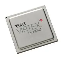
XCVU9P-2FLGA2104I – Integrated Circuits, Embedded, FPGAs (Field Programmable Gate Array)
The Xilinx® Virtex® UltraScale+™ FPGAs are available in -3, -2, -1 speed grades, with -3E devices having the highest performance. The -2LE devices can operate at a VCCINT voltage at 0.85V or 0.72V and provide lower maximum static power. When operated at VCCINT = 0.85V, using -2LE devices, the speed specification for the L devices is the same as the -2I speed grade. When operated at VCCINT = 0.72V, the -2LE performance and static and dynamic power is reduced. DC and AC characteristics are specified in extended (E), industrial (I), and military (M) temperature ranges. Except the operating temperature range or unless otherwise noted, all the DC and AC electrical parameters are the same for a particular speed grade (that is, the timing characteristics of a -1 speed grade extended device are the same as for a -1 speed grade industrial device). However, only selected speed grades and/or devices are available in each temperature range.
-

XCVU9P-2FLGB2104I – Integrated Circuits, Embedded, Field Programmable Gate Array
The Xilinx® Virtex® UltraScale+™ FPGAs are available in -3, -2, -1 speed grades, with -3E devices having the highest performance. The -2LE devices can operate at a VCCINT voltage at 0.85V or 0.72V and provide lower maximum static power. When operated at VCCINT = 0.85V, using -2LE devices, the speed specification for the L devices is the same as the -2I speed grade. When operated at VCCINT = 0.72V, the -2LE performance and static and dynamic power is reduced. DC and AC characteristics are specified in extended (E), industrial (I), and military (M) temperature ranges. Except the operating temperature range or unless otherwise noted, all the DC and AC electrical parameters are the same for a particular speed grade (that is, the timing characteristics of a -1 speed grade extended device are the same as for a -1 speed grade industrial device). However, only selected speed grades and/or devices are available in each temperature range. The XQ references in this data sheet are specific to the devices available in XQ Ruggedized packages. See the Defense-Grade UltraScale Architecture Data Sheet: Overview (DS895) for further information on XQ Defensegrade part numbers, packages, and ordering information.
-

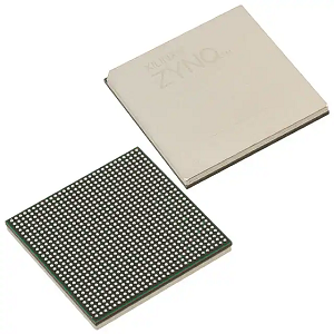
XCZU6CG-2FFVC900I – Integrated Circuits, Embedded, System On Chip (SoC)
The Zynq® UltraScale+™ MPSoC family is based on the UltraScale™ MPSoC architecture. This family of products integrates a feature-rich 64-bit quad-core or dual-core Arm® Cortex®-A53 and dual-core Arm Cortex-R5F based processing system (PS) and Xilinx programmable logic (PL) UltraScale architecture in a single device. Also included are on-chip memory, multiport external memory interfaces, and a rich set of peripheral connectivity interfaces.
-
TPS62202DBVR – Integrated Circuits (ICs), Power Management (PMIC), Voltage Regulators – DC DC Switching Regulators
The TPS6220x device is a synchronous step-down converter operating with typically 1-MHz fixed frequency pulse width modulation (PWM) at moderate to heavy load currents and in power save mode operating with pulse frequency modulation (PFM) at light load currents. During PWM operation the converter uses a unique fast response, voltage mode, controller scheme with input voltage feed forward. This achieves good line and load regulation and allows the use of small ceramic input and output capacitors. At the beginning of each clock cycle initiated by the clock signal (S), the P-channel MOSFET switch is turned on, and the inductor current ramps up until the comparator trips and the control logic turns off the switch. The current limit comparator also turns off the switch in case the current limit of the P-channel switch is exceeded. Then the N-channel rectifier switch is turned on and the inductor current ramps down. The next cycle is initiated by the clock signal again turning off the N-channel rectifier and turning on the P-channel switch. The GM amplifier and input voltage determines the rise time of the Sawtooth generator; therefore any change in input voltage or output voltage directly controls the duty cycle of the converter. This gives a very good line and load transient regulation.
-

TPL5010DDCR – Integrated Circuits (ICs), Clock/Timing, Programmable Timers and Oscillators
The TPL5010 Nano Timer is an ultra-low power timer with a watchdog feature designed for system wake up in duty-cycled, battery-powered applications such as those in IoT. Many of these applications require the use of a μC, so it is desirable to keep the μC in a low power mode to maximize current savings, waking up only during certain time intervals to collect data or service an interrupt. Although the internal timer of the μC can be used for system wake-up, it can single handedly consume microamps of total system current. -
TLV62569PDDCR – Integrated Circuits (ICs), Power Management (PMIC), Voltage Regulators – DC DC Switching Regulators
The TLV62569 device is a synchronous step-down buck DC-DC converter optimized for high efficiency and compact solution size. The device integrates switches capable of delivering an output current up to 2 A.
At medium to heavy loads, the device operates in pulse width modulation (PWM) mode with 1.5-MHz switching frequency. At light load, the device automatically enters Power Save Mode (PSM) to maintain high efficiency over the entire load current range. In shutdown, the current consumption is reduced to less than 2 μA.
The TLV62569 provides an adjustable output voltage via an external resistor divider. An internal soft start circuit limits the inrush current during startup. Other features like over current
protection, thermal shutdown protection and power good are built-in. The device is available in a SOT23 and SOT563 package.
-

TLV62080DSGR – Integrated Circuits (ICs), Power Management (PMIC), Voltage Regulators – DC DC Switching Regulators
The TLV6208x family devices are small buck converters with few external components, enabling cost effective solutions. They are synchronous step down converters with an input voltage range of 2.5 and 2.7 (2.5 V for TLV62080, 2.7 V for TLV62084x) to 6 V. The TLV6208x devices focus on high efficiency step down conversion over a wide output current range. At medium to heavy loads, the TLV6208x converters operate in PWM mode and automatically enter power save mode operation at light-load currents to maintain high efficiency over the entire load current range.To address the requirements of system power rails, the internal compensation circuit allows a wide range of external output capacitor values. With the DCS Control™ (Direct Control with Seamless transition into Power save mode) architecture excellent load transient performance and output voltage regulation accuracy are achieved. The devices are available in 2-mm × 2-mm WSON package with Thermal Pad. -
XCKU15P-2FFVE1760E 100% new and original stock
This brand of FPGA series has excellent cost performance, performance, power consumption, and provides high-end functions, such as transceivers, memory interface line rates, 100G connection chips, etc. FPGA selectable -3, -2, -1 speed grades. This series is ideal for packet processing, DSP functions, and applications such as wireless MIMO technology, Nx100G networks and data centers. The device adopts UltraScale™ architecture, which has ultra-high performance, with on-chip UltraRAM memory, which can reduce BOM cost, and can cooperate with high-performance peripherals to create cost-effective systems. FPGAs have a variety of power supply options, balancing system performance with required power.
-
LCMXO2-2000HC-4TG100I FPGA CPLD MachXO2-2000HC 2.5V/3.3V
CPLD MachXO2-2000HC 2.5V/3.3V TQFP100 LCMXO2-2000HC-4TG100I, CPLD MachXO2 Flash 79 I/O, 2112 Labs, 7.24ns, ISP, 2.375 → 3.465 V 100-Pin TQFP
-
TPS54360BQDDARQ1 New and Original Step Down DC-DC Converter with Eco-mode™ Automotive
The TPS54360B-Q1 is a 60-V 3.5-A step-down regulator with an integrated high-side MOSFET. It is qualified for automotive application.
