


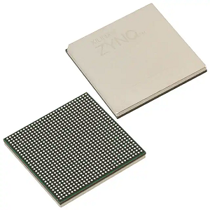
XC7Z100-2FFG900I – Integrated Circuits, Embedded, System On Chip (SoC)
Product Attributes
| TYPE | DESCRIPTION |
| Category | Integrated Circuits (ICs) |
| Mfr | AMD |
| Series | Zynq®-7000 |
| Package | Tray |
| Product Status | Active |
| Architecture | MCU, FPGA |
| Core Processor | Dual ARM® Cortex®-A9 MPCore™ with CoreSight™ |
| Flash Size | - |
| RAM Size | 256KB |
| Peripherals | DMA |
| Connectivity | CANbus, EBI/EMI, Ethernet, I²C, MMC/SD/SDIO, SPI, UART/USART, USB OTG |
| Speed | 800MHz |
| Primary Attributes | Kintex™-7 FPGA, 444K Logic Cells |
| Operating Temperature | -40°C ~ 100°C (TJ) |
| Package / Case | 900-BBGA, FCBGA |
| Supplier Device Package | 900-FCBGA (31x31) |
| Number of I/O | 212 |
| Base Product Number | XC7Z100 |
Documents & Media
| RESOURCE TYPE | LINK |
| Datasheets | XC7Z030,35,45,100 Datasheet |
| Product Training Modules | Powering Series 7 Xilinx FPGAs with TI Power Management Solutions |
| Environmental Information | Xiliinx RoHS Cert |
| Featured Product | All Programmable Zynq®-7000 SoC |
| PCN Design/Specification | Mult Dev Material Chg 16/Dec/2019 |
| PCN Packaging | Mult Devices 26/Jun/2017 |
Environmental & Export Classifications
| ATTRIBUTE | DESCRIPTION |
| RoHS Status | ROHS3 Compliant |
| Moisture Sensitivity Level (MSL) | 4 (72 Hours) |
| REACH Status | REACH Unaffected |
| ECCN | 3A991D |
| HTSUS | 8542.39.0001 |
SoC
Basic SoC architecture
A typical system-on-chip architecture consists of the following components:
- At least one microcontroller (MCU) or microprocessor (MPU) or digital signal processor (DSP), but there can be multiple processor cores.
- The memory may be one or more of RAM, ROM, EEPROM and flash memory.
- Oscillator and phase-locked loop circuitry for providing time pulse signals.
- Peripherals consisting of counters and timers, power supply circuits.
- Interfaces for different standards of connectivity such as USB, FireWire, Ethernet, universal asynchronous transceiver and serial peripheral interfaces, etc..
- ADC/DAC for conversion between digital and analogue signals.
- Voltage regulation circuits and voltage regulators.
Limitations of SoCs
Currently, the design of SoC communication architectures is relatively mature. Most chip companies use SoC architectures for their chip manufacturing. However, as commercial applications continue to pursue instruction co-existence and predictability, the number of cores integrated into the chip will continue to increase and bus-based SoC architectures will become increasingly difficult to meet the growing demands of computing. The main manifestations of this are
1. poor scalability. soC system design starts with a system requirements analysis, which identifies the modules in the hardware system. In order for the system to work correctly, the position of each physical module in the SoC on the chip is relatively fixed. Once the physical design has been completed, modifications have to be made, which can effectively be a redesign process. On the other hand, SoCs based on bus architecture are limited in the number of processor cores that can be extended on them due to the inherent arbitration communication mechanism of the bus architecture, i.e. only one pair of processor cores can communicate at the same time.
2. With a bus architecture based on an exclusive mechanism, each functional module in a SoC can only communicate with other modules in the system once it has gained control of the bus. As a whole, when a module acquires bus arbitration rights for communication, other modules in the system must wait until the bus is free.
3. Single clock synchronisation problem. The bus structure requires global synchronisation, however, as the process feature size becomes smaller and smaller, the operating frequency rises rapidly, reaching 10GHz later, the impact caused by the connection delay will be so serious that it is impossible to design a global clock tree, and because of the huge clock network, its power consumption will occupy most of the total power consumption of the chip.
-
Original new BSZ100 Transistor PG-TSDSON-8 BSZ1...
-
Brand new Original Electronic components IC Chi...
-

HFBR-782BZ New original electronic components H...
-
EP2AGX65DF25C6G new&original ic chips inte...
-
JXSQ New and Original IC chips REG BUCK ADJ 3.5...
-

New and Original Integrated Circuit Hot Sale El...