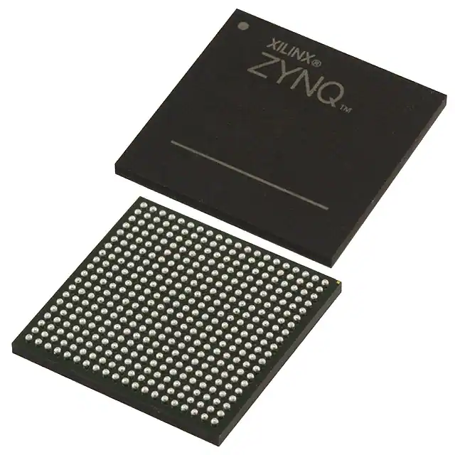
XCVU9P-2FLGB2104I – Integrated Circuits, Embedded, Field Programmable Gate Array
Product Attributes
| TYPE | DESCRIPTION |
SELECT |
| Category | Integrated Circuits (ICs) | |
| Mfr | AMD | |
| Series | Virtex® UltraScale+™ | |
| Package | Tray | |
| Product Status | Active | |
| DigiKey Programmable | Not Verified | |
| Number of LABs/CLBs | 147780 | |
| Number of Logic Elements/Cells | 2586150 | |
| Total RAM Bits | 391168000 | |
| Number of I/O | 702 | |
| Voltage - Supply | 0.825V ~ 0.876V | |
| Mounting Type | Surface Mount | |
| Operating Temperature | -40°C ~ 100°C (TJ) | |
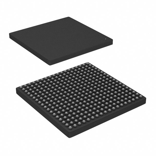
| Package / Case | 2104-BBGA, FCBGA | |
| Supplier Device Package | 2104-FCBGA (47.5x47.5) | |
| Base Product Number | XCVU9 |
Documents & Media
| RESOURCE TYPE | LINK |
| Datasheets | Virtex UltraScale+ FPGA Datasheet |
| Environmental Information | Xiliinx RoHS Cert |
| EDA Models | XCVU9P-2FLGB2104I by Ultra Librarian |
Environmental & Export Classifications
| ATTRIBUTE | DESCRIPTION |
| RoHS Status | ROHS3 Compliant |
| Moisture Sensitivity Level (MSL) | 4 (72 Hours) |
| ECCN | 3A001A7B |
| HTSUS | 8542.39.0001 |
FPGAs
FPGA (Field Programmable Gate Array) is a further development of programmable devices such as PAL (Programmable Array Logic) and GAL (General Array Logic). It emerged as a semi-custom circuit in the field of Application Specific Integrated Circuits (ASICs), addressing the shortcomings of custom circuits and overcoming the limited number of gates of the original programmable devices.
FPGA design is not simply the study of chips, but mainly the use of FPGA patterns for the design of products in other industries. Unlike ASICs, FPGAs are more widely used in the communications industry. Through the analysis of the global FPGA product market and related suppliers, combined with the current actual situation in China and the leading domestic FPGA products can be found in the future development direction of the relevant technology, has a very important role in promoting the overall improvement of China's science and technology level.
In contrast to the traditional model of chip design, FPGA chips are not limited to research and design chips, but can be optimised for a wide range of products with a specific chip model. From the point of view of the device, the FPGA itself constitutes a typical integrated circuit in a semi-customised circuit, containing digital management modules, embedded units, output units and input units. On this basis, it is necessary to focus on a comprehensive chip optimisation of the FPGA chip, adding new chip functions by improving the current chip design, thus simplifying the overall chip structure and improving performance.
Basic structure:
FPGA devices belong to a kind of semi-custom circuit in special-purpose integrated circuits, which are programmable logic arrays and can effectively solve the problem of low gate circuit number of the original devices. the basic structure of FPGA includes programmable input and output units, configurable logic blocks, digital clock management modules, embedded block RAM, wiring resources, embedded dedicated hard cores, and bottom embedded functional units. FPGAs are widely used in the field of digital circuit design due to their rich wiring resources, repeatable programming and high integration, and low investment. FPGA design flow includes algorithm design, code simulation and design, board debugging, the designer and the actual requirements to establish the algorithm architecture, use EDA to establish the design scheme or HD to write the design code, ensure through code simulation The design solution meets the actual requirements, and finally the board-level debugging is carried out, using the configuration circuit to download the relevant files into the FPGA chip to verify the actual operation.