


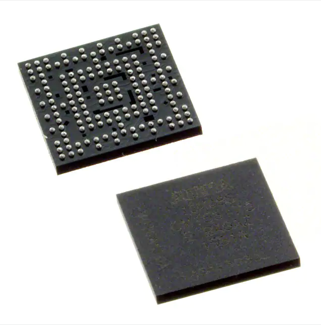
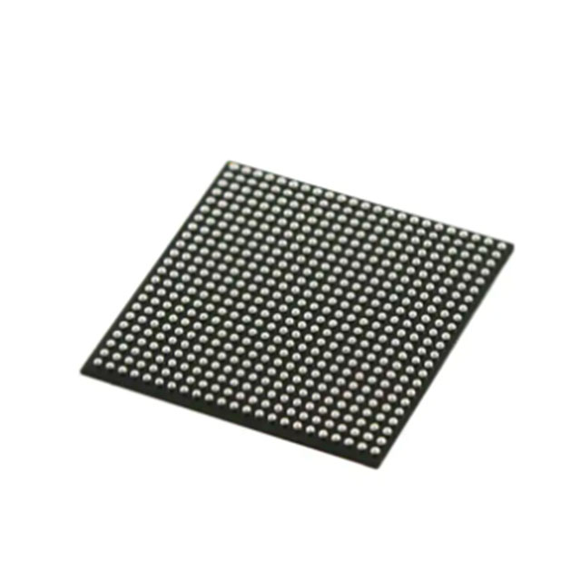
Original support BOM chip electronic components EP4SE360F35C3G IC FPGA 744 I/O 1152FBGA
Product Attributes
| TYPE | DESCRIPTION |
| Category | Integrated Circuits (ICs) Embedded FPGAs (Field Programmable Gate Array) |
| Mfr | Intel |
| Series | * |
| Package | Tray |
| Standard Package | 24 |
| Product Status | Active |
| Base Product Number | EP4SE360 |
Intel reveals 3D chip details: capable of stacking 100 billion transistors, plans to launch in 2023
The 3D stacked chip is Intel’s new direction to challenge Moore’s Law by stacking the logic components in the chip to dramatically increase the density of CPUs, GPUs, and AI processors. With chip processes nearing a standstill, this may be the only way to continue to improve performance.
Recently, Intel presented new details of its 3D Foveros chip design for the upcoming Meteor Lake, Arrow Lake, and Lunar Lake chips at the semiconductor industry conference Hot Chips 34.
Recent rumors have suggested that Intel’s Meteor Lake will be delayed due to the need to switch Intel’s GPU tile/chipset from the TSMC 3nm node to the 5nm node. While Intel still hasn’t shared information about the specific node it will use for the GPU, a company representative said that the planned node for the GPU component has not changed and that the processor is on track for an on-time release in 2023.
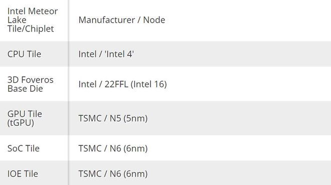
Notably, this time Intel will only produce one of the four components (the CPU part) used to build its Meteor Lake chips – TSMC will produce the other three. Industry sources point out that the GPU tile is TSMC N5 (5nm process).
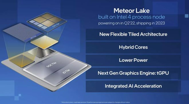
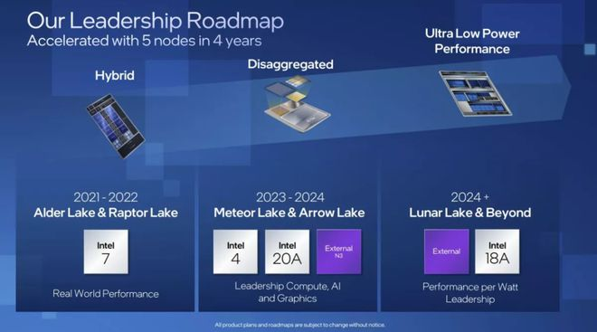
Intel has shared the latest images of the Meteor Lake processor, which will use Intel’s 4 process node (7nm process) and will first hit the market as a mobile processor with six large cores and two small cores. The Meteor Lake and Arrow Lake chips cover the needs of the mobile and desktop PC markets, while Lunar Lake will be used in thin and light notebooks, covering the 15W and below market.
Advances in packaging and interconnects are rapidly changing the face of modern processors. Both are now as important as the underlying process node technology – and arguably more important in some ways.
Many of Intel’s disclosures on Monday focused on its 3D Foveros packaging technology, which will be used as the basis for its Meteor Lake, Arrow Lake, and Lunar Lake processors for the consumer market. This technology allows Intel to vertically stack small chips on a unified base chip with Foveros interconnects. Intel is also using Foveros for its Ponte Vecchio and Rialto Bridge GPUs and Agilex FPGAs, so it could be considered the underlying technology for several of the company’s next-generation products.
Intel has previously brought 3D Foveros to market on its low-volume Lakefield processors, but the 4-tile Meteor Lake and nearly 50-tile Ponte Vecchio are the company’s first chips to be mass-produced with the technology. After Arrow Lake, Intel will transition to the new UCI interconnect, which will allow it to enter the chipset ecosystem using a standardized interface.
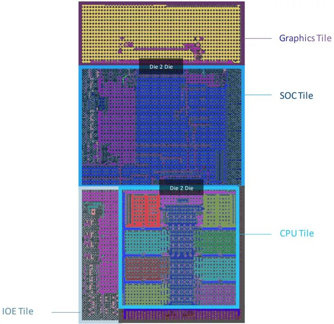
Intel has revealed that it will place four Meteor Lake chipsets (called “tiles/tiles” in Intel’s parlance) on top of the passive Foveros intermediate layer/base tile. The base tile in Meteor Lake is different from the one in Lakefield, which can be considered an SoC in a sense. 3D Foveros packaging technology also supports an active intermediary layer. Intel says it uses a low-cost and low-power optimized 22FFL process (the same as Lakefield) to manufacture the Foveros interposer layer. Intel also offers an updated ‘Intel 16′ variant of this node for its foundry services, but it is not clear which version of the Meteor Lake base tile Intel will use.
Intel will install compute modules, I/O blocks, SoC blocks, and graphics blocks (GPUs) using Intel 4 processes on this intermediary layer. All of these units are designed by Intel and use Intel architecture, but TSMC will OEM the I/O, SoC, and GPU blocks in them. This means that Intel will only produce the CPU and Foveros blocks.
Industry sources leak that the I/O die and SoC are made on TSMC’s N6 process, while the tGPU uses TSMC N5. (It is worth noting that Intel refers to the I/O tile as the ‘I/O Expander’, or IOE)
Future nodes on the Foveros roadmap include 25 and 18-micron pitches. Intel says it is even theoretically possible to achieve 1-micron bump spacing in the future using Hybrid Bonded Interconnects (HBI).
-
IPD031N06L3G new original Electronic Components...
-
Original Electronic Component 5M570ZT144C5N EP2...
-
LMR16030SDDAR China Original Integrated Circuit...
-
.jpg)
3-A Synchronous Step-Down Voltage Converter Int...
-
New Electronic Component 10M02SCM153I7G EN6337Q...
-
Original Electronic Component EP4CGX50CF23C8N E...