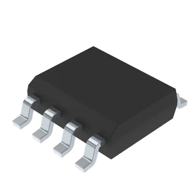
Brand new genuine original IC stock Electronic Components Ic Chip Support BOM Service DS90UB953TRHBRQ1
Product Attributes
| TYPE | DESCRIPTION |
| Category | Integrated Circuits (ICs) |
| Mfr | Texas Instruments |
| Series | Automotive, AEC-Q100 |
| Package | Tape & Reel (TR)
Cut Tape (CT) Digi-Reel® |
| SPQ | 3000T&R |
| Product Status | Active |
| Function | Serializer |
| Data Rate | 4.16Gbps |
| Input Type | CSI-2, MIPI |
| Output Type | FPD-Link III, LVDS |
| Number of Inputs | 1 |
| Number of Outputs | 1 |
| Voltage - Supply | 1.71V ~ 1.89V |
| Operating Temperature | -40°C ~ 105°C |
| Mounting Type | Surface Mount, Wettable Flank |
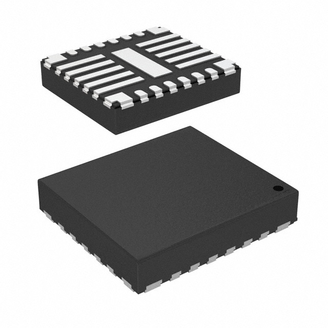
| Package / Case | 32-VFQFN Exposed Pad |
| Supplier Device Package | 32-VQFN (5x5) |
| Base Product Number | DS90UB953 |
1.Why silicon for chips? Are there materials that can replace it in the future?
The raw material for chips is wafers, which are composed of silicon. There is a misconception that "sand can be used to make chips", but this is not the case. The main chemical component of sand is silicon dioxide, and the main chemical component of glass and wafers is also silicon dioxide. The difference, however, is that glass is polycrystalline silicon, and heating sand at high temperatures yields polycrystalline silicon. Wafers, on the other hand, are monocrystalline silicon, and if they are made from the sand they need to be further transformed from polycrystalline silicon to monocrystalline silicon.
What exactly is silicon and why can it be used to make chips, we will reveal this in this article one by one.
The first thing we need to understand is that silicon material is not a direct jump to the chip step, silicon is refined from quartz sand out of the element silicon, silicon element proton number than the element aluminum one more, than the element phosphorus one less, it is not only the material basis of modern electronic computing devices but also people looking for extraterrestrial life one of the basic possible elements. Usually, when silicon is purified and refined (99.999%), it can be manufactured into silicon wafers, which are then sliced into wafers. The thinner the wafer, the lower the cost of manufacturing the chip, but the higher the requirements for the chip process.
Three important steps in turning silicon into wafers
Specifically, the transformation of silicon into wafers can be divided into three steps: silicon refining and purification, single crystal silicon growth, and wafer forming.
In nature, silicon is generally found in the form of silicate or silicon dioxide in sand and gravel. The raw material is placed in an electric arc furnace at 2000°C and in the presence of a carbon source, and the high temperature is used to react silicon dioxide with carbon (SiO2 + 2C = Si + 2CO) to obtain metallurgical grade silicon (purity around 98%). However, this purity is not sufficient for the preparation of electronic components, so it has to be further purified. The crushed metallurgical grade silicon is chlorinated with gaseous hydrogen chloride to produce liquid silane, which is then distilled and chemically reduced by a process that yields high purity polysilicon with a purity of 99.9999999999% as electronic grade silicon.
So how do you get monocrystalline silicon from polycrystalline silicon? The most common method is the direct pulling method, where polysilicon is placed in a quartz crucible and heated with a temperature of 1400°C held at the periphery, which produces a polysilicon melt. Of course, this is preceded by dipping a seed crystal into it and having the drawing rod carry the seed crystal in the opposite direction while slowly and vertically pulling it upwards from the silicon melt. The polycrystalline silicon melt sticks to the bottom of the seed crystal and grows upwards in the direction of the seed crystal lattice, which after being pulled out and cooled grows into a single crystal bar with the same lattice orientation as the inner seed crystal. Finally, the single-crystal wafers are tumbled, cut, ground, chamfered, and polished to produce the all-important wafers.
Depending on the cut size, silicon wafers can be classified as 6", 8", 12", and 18". The larger the size of the wafer, the more chips can be cut out of each wafer, and the lower the cost per chip.
2.Three important steps in the transformation of silicon into wafers
Specifically, the transformation of silicon into wafers can be divided into three steps: silicon refining and purification, single crystal silicon growth, and wafer forming.
In nature, silicon is generally found in the form of silicate or silicon dioxide in sand and gravel. The raw material is placed in an electric arc furnace at 2000°C and in the presence of a carbon source, and the high temperature is used to react silicon dioxide with carbon (SiO2 + 2C = Si + 2CO) to obtain metallurgical grade silicon (purity about 98%). However, this purity is not sufficient for the preparation of electronic components, so it has to be further purified. The crushed metallurgical grade silicon is chlorinated with gaseous hydrogen chloride to produce liquid silane, which is then distilled and chemically reduced by a process that yields high purity polysilicon with a purity of 99.9999999999% as electronic grade silicon.
So how do you get monocrystalline silicon from polycrystalline silicon? The most common method is the direct pulling method, where polysilicon is placed in a quartz crucible and heated with a temperature of 1400°C held at the periphery, which produces a polysilicon melt. Of course, this is preceded by dipping a seed crystal into it and having the drawing rod carry the seed crystal in the opposite direction while slowly and vertically pulling it upwards from the silicon melt. The polycrystalline silicon melt sticks to the bottom of the seed crystal and grows upwards in the direction of the seed crystal lattice, which after being pulled out and cooled grows into a single crystal bar with the same lattice orientation as the inner seed crystal. Finally, the single-crystal wafers are tumbled, cut, ground, chamfered, and polished to produce the all-important wafers.
Depending on the cut size, silicon wafers can be classified as 6", 8", 12", and 18". The larger the size of the wafer, the more chips can be cut out of each wafer, and the lower the cost per chip.
Why is silicon the most suitable material for making chips?
Theoretically, all semiconductors can be used as chip materials, but the main reasons why silicon is the most suitable material for making chips are as follows.
1, according to the ranking of the earth's elemental content, in order: oxygen > silicon > aluminum > iron > calcium > sodium > potassium ...... can see that silicon ranked second, the content is huge, which also allows the chip to have an almost inexhaustible supply of raw materials.
2, silicon element chemical properties and material properties are very stable, the earliest transistor is the use of semiconductor materials germanium to make, but because the temperature exceeds 75 ℃, the conductivity will be a large change, made into a PN junction after the reverse leakage current of germanium than silicon, so the selection of silicon element as a chip material is more appropriate;
3, silicon element purification technology is mature, and low cost, nowadays the purification of silicon can reach 99.9999999999%.
4, silicon material itself is non-toxic and harmless, which is also one of the important reasons why it is chosen as the manufacturing material for chips.