Semiconductors Electronic Components TPS7A5201QRGRRQ1 Ic Chips BOM service One spot buy

Product Attributes
| TYPE | DESCRIPTION |
| Category | Integrated Circuits (ICs) |
| Mfr | Texas Instruments |
| Series | Automotive, AEC-Q100 |
| Package | Tape & Reel (TR)
Cut Tape (CT) Digi-Reel® |
| SPQ | 3000T&R |
| Product Status | Active |
| Output Configuration | Positive |
| Output Type | Adjustable |
| Number of Regulators | 1 |
| Voltage - Input (Max) | 6.5V |
| Voltage - Output (Min/Fixed) | 0.8V |
| Voltage - Output (Max) | 5.2V |
| Voltage Dropout (Max) | 0.3V @ 2A |
| Current - Output | 2A |
| PSRR | 42dB ~ 25dB (10kHz ~ 500kHz) |
| Control Features | Enable |
| Protection Features | Over Temperature, Reverse Polarity |
| Operating Temperature | -40°C ~ 150°C (TJ) |
| Mounting Type | Surface Mount |
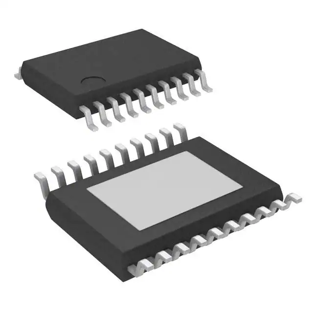
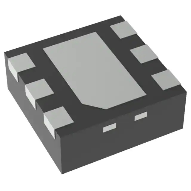
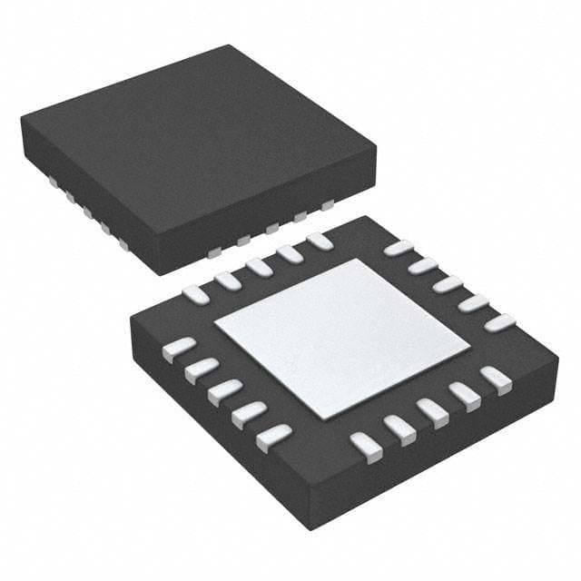
| Package / Case | 20-VFQFN Exposed Pad |
| Supplier Device Package | 20-VQFN (3.5x3.5) |
| Base Product Number | TPS7A5201 |
Overview of chips
(i) What is a chip
The integrated circuit, abbreviated as IC; or microcircuit, microchip, the chip is a way of miniaturizing circuits (mainly semiconductor devices, but also passive components, etc.) in electronics, and is often manufactured on the surface of semiconductor wafers.
(ii) Chip manufacturing process
The complete chip fabrication process includes chip design, wafer fabrication, package fabrication, and testing, among which the wafer fabrication process is particularly complex.
First is the chip design, according to the design requirements, the generated "pattern", the raw material of the chip is the wafer.
The wafer is made of silicon, which is refined from quartz sand. The wafer is the silicon element purified (99.999%), then the pure silicon is made into silicon rods, which become the material for manufacturing quartz semiconductors for integrated circuits, which are sliced into wafers for chip production. The thinner the wafer, the lower the cost of production, but the more demanding the process.
Wafer coating
Wafer coating is resistant to oxidation and temperature resistance and is a type of photoresist.
Wafer photolithography development and etching
The basic flow of the photolithography process is shown in the diagram below. First, a layer of photoresist is applied to the surface of the wafer (or substrate) and dried. After drying, the wafer is transferred to the lithography machine. Light is passed through a mask to project the pattern on the mask onto the photoresist on the wafer surface, enabling exposure and stimulating the photochemical reaction. The exposed wafers are then baked a second time, known as post-exposure baking, where the photochemical reaction is more complete. Finally, the developer is sprayed onto the photoresist on the wafer surface to develop the exposed pattern. After development, the pattern on the mask is left on the photoresist.
Gluing, baking, and developing are all done in the screed developer and the exposure is done in the photolithograph. The screed developer and the lithography machine are generally operated inline, with the wafers being transferred between the units and the machine using a robot. The entire exposure and development system is closed and the wafers are not directly exposed to the surrounding environment to reduce the impact of harmful components in the environment on the photoresist and photochemical reactions.
Doping with impurities
Implanting ions into the wafer to produce the corresponding P and N-type semiconductors.
Wafer testing
After the above processes, a lattice of dice is formed on the wafer. The electrical characteristics of each die are checked using a pin test.
Packaging
The manufactured wafers are fixed, bound to pins, and made into different packages according to the requirements, which is why the same chip core can be packaged in different ways. For example, DIP, QFP, PLCC, QFN, and so on. Here it is mainly determined by the user's application habits, application environment, market format, and other peripheral factors.
Testing, packaging
After the above process, the chip production is complete. This step is to test the chip, remove defective products and package it.
The relationship between wafers and chips
A chip is made up of more than one semiconductor device. Semiconductors are generally diodes, triodes, field effect tubes, small power resistors, inductors, capacitors, and so on.
It is the use of technical means to change the concentration of free electrons in the atomic nucleus in a circular well to change the physical properties of the atomic nucleus to produce a positive or negative charge of the many (electrons) or few (holes) to form various semiconductors.
Silicon and germanium are commonly used semiconductor materials and their properties and materials are readily available in large quantities and at a low cost for use in these technologies.
A silicon wafer is made up of a large number of semiconductor devices. The function of a semiconductor is, of course, to form a circuit as required and to exist in the silicon wafer.