Electronic Components IC Chips Integrated Circuits BOM service TPS4H160AQPWPRQ1

Product Attributes
| TYPE | DESCRIPTION |
| Category | Integrated Circuits (ICs) |
| Mfr | Texas Instruments |
| Series | Automotive, AEC-Q100 |
| Package | Tape & Reel (TR)
Cut Tape (CT) Digi-Reel® |
| SPQ | 2000T&R |
| Product Status | Active |
| Switch Type | General Purpose |
| Number of Outputs | 4 |
| Ratio - Input:Output | 1:1 |
| Output Configuration | High Side |
| Output Type | N-Channel |
| Interface | On/Off |
| Voltage - Load | 3.4V ~ 40V |
| Voltage - Supply (Vcc/Vdd) | Not Required |
| Current - Output (Max) | 2.5A |
| Rds On (Typ) | 165mOhm |
| Input Type | Non-Inverting |
| Features | Status Flag |
| Fault Protection | Current Limiting (Fixed), Over Temperature |
| Operating Temperature | -40°C ~ 125°C (TA) |
| Mounting Type | Surface Mount |
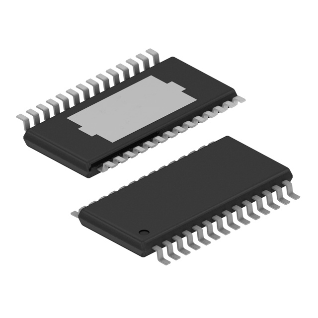
| Supplier Device Package | 28-HTSSOP |
| Package / Case | 28-PowerTSSOP (0.173", 4.40mm Width) |
| Base Product Number | TPS4H160 |
The relationship between wafers and chips
A chip is made up of more than N semiconductor devices Semiconductors are generally diodes triodes field effect tubes small power resistors inductors capacitors etc.
It is the use of technical means to change the concentration of free electrons in the atomic nucleus in a circular well to change the physical properties of the atomic nucleus to produce a positive or negative charge of the many (electrons) or few (holes) to form various semiconductors.
Silicon and germanium are commonly used semiconductor materials and their properties and materials are easily and inexpensively available in large quantities for use in these technologies.
A silicon wafer is made up of a large number of semiconductor devices. The function of the wafer is, of course, to form a circuit out of the semiconductors that are present in the wafer as required.
The relationship between wafers and chips - how many wafers are in a chip
This depends on the size of your die, the size of your wafer, and the yield rate.
At present, the industry's so-called 6", 12" or 18" wafers are short for wafer diameter, but the inches are an estimate. The actual wafer diameter is divided into 150mm, 300mm and 450mm, and 12" is equal to 305mm, so it is called 12" wafer for convenience.
A complete wafer
Explanation: A wafer is the wafer shown in the picture and is made of pure silicon (Si). A wafer is a small piece of the silicon wafer, known as a die, which is packaged as a pellet. A wafer containing a Nand Flash wafer, the wafer is first cut, then tested and the intact, stable, full-capacity die is removed and packaged to form the Nand Flash chip that you see every day.
What remains on the wafer is then either unstable, partially damaged, and therefore under-capacity, or completely damaged. The original manufacturer, in consideration of quality assurance, will declare such dead dead and strictly define them as scrap for total scrap disposal.
The relationship between die and wafer
After the die is cut down, the original wafer becomes what is shown in the picture below, which is the Downgrade Flash Wafer left over.
Screened wafer
These residual dies are sub-standard wafers. The part that was removed, the black part, is the qualified die and will be packaged and made into finished NAND pellets by the original manufacturer, while the unqualified part, the part left in the picture, will be disposed of as scrap.