


SN74ACT244PWR 8-ch, 4.5-V to 5.5-V buffers with TTL-compatible CMOS inputs and 3-state outputs

Product Attributes
| EU RoHS | Compliant |
| ECCN (US) | EAR99 |
| Part Status | Active |
| HTS | 8542.39.00.01 |
| Automotive | No |
| PPAP | No |
| Logic Family | ACT |
| Logic Function | Buffer/Line Driver |
| Number of Elements per Chip | 2 |
| Number of Channels per Chip | 8 |
| Number of Inputs per Chip | 8 |
| Number of Input Enables per Chip | 0 |
| Number of Outputs per Chip | 8 |
| Number of Output Enables per Chip | 2 Low |
| Bus Hold | No |
| Polarity | Non-Inverting |
| Maximum Propagation Delay Time @ Maximum CL (ns) | 9@4.5V to 5.5V |
| Absolute Propagation Delay Time (ns) | 10.5 |
| Process Technology | CMOS |
| Input Signal Type | Single-Ended |
| Output Type | 3-State |
| Maximum Low Level Output Current (mA) | 24 |
| Maximum High Level Output Current (mA) | -24 |
| Minimum Operating Supply Voltage (V) | 4.5 |
| Typical Operating Supply Voltage (V) | 5 |
| Maximum Operating Supply Voltage (V) | 5.5 |
| Tolerant I/Os (V) | 5.5 Inputs |
| Maximum Quiescent Current (uA) | 4 |
| Propagation Delay Test Condition (pF) | 50 |
| Minimum Operating Temperature (°C) | -40 |
| Maximum Operating Temperature (°C) | 85 |
| Supplier Temperature Grade | Commercial |
| Packaging | Tape and Reel |
| Mounting | Surface Mount |
| Package Height | 1.05(Max) |
| Package Width | 4.5(Max) |
| Package Length | 6.6(Max) |
| PCB changed | 20 |
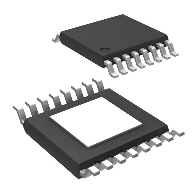
| Standard Package Name | SOP |
| Supplier Package | TSSOP |
| Pin Count | 20 |
| Lead Shape | Gull-wing |
Detailed Introduction
These SNx4ACT244 octal buffers and drivers are designed specifically to improve the performance and density of 3-state memory address drivers, clock drivers, and bus-oriented receivers and transmitters. The SNx4ACT244 devices are organized as two 4-bit buffers and drivers with separate output-enable (OE) inputs. When OE is low, the device passes non inverted data from the A inputs to the Y outputs. When OE is high, the outputs are in the high impedance state.

Write your message here and send it to us
-
New And Original Integrated Circuit IC multiple...
-

Electronic Components IC Chips Integrated Circu...
-
Semicon Original Electric Components Electronic...
-
AMC1311QDWVRQ1 High Quality Ic Chips Electronic...
-
.png)
Merrillchip New & Original in stock Electr...
-
Orignal DS90UB935TRHBRRQ1 Intergrated Circuit I...