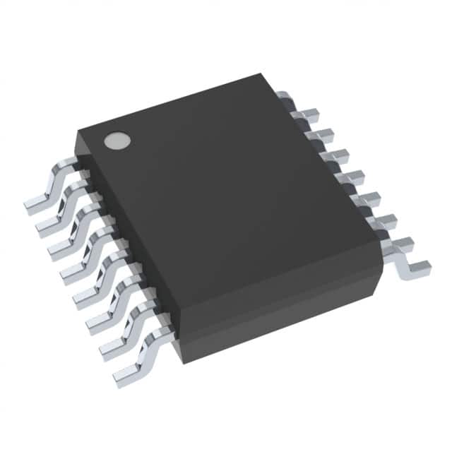
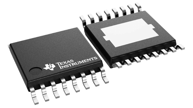
LM46002AQPWPRQ1 package HTSSOP16 integrated circuit IC chip new original spot electronics components
Product Attributes
| TYPE | DESCRIPTION |
| Category | Integrated Circuits (ICs) |
| Mfr | Texas Instruments |
| Series | Automotive, AEC-Q100, SIMPLE SWITCHER® |
| Package | Tape & Reel (TR)
Cut Tape (CT) Digi-Reel® |
| SPQ | 2000T&R |
| Product Status | Active |
| Function | Step-Down |
| Output Configuration | Positive |
| Topology | Buck |
| Output Type | Adjustable |
| Number of Outputs | 1 |
| Voltage - Input (Min) | 3.5V |
| Voltage - Input (Max) | 60V |
| Voltage - Output (Min/Fixed) | 1V |
| Voltage - Output (Max) | 28V |
| Current - Output | 2A |
| Frequency - Switching | 200kHz ~ 2.2MHz |
| Synchronous Rectifier | Yes |
| Operating Temperature | -40°C ~ 125°C (TJ) |
| Mounting Type | Surface Mount |
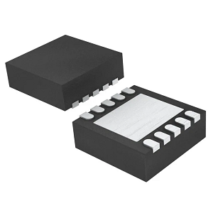
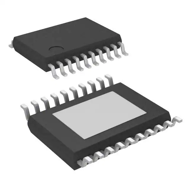
| Package / Case | 16-TSSOP (0.173", 4.40mm Width) Exposed Pad |
| Supplier Device Package | 16-HTSSOP |
| Base Product Number | LM46002 |
Chip production process
The complete chip fabrication process includes chip design, wafer production, chip packaging, and chip testing, among which the wafer production process is particularly complex.
The first step is the chip design, which is based on the design requirements, such as functional objectives, specifications, circuit layout, wire winding and detailing, etc. The "design drawings" are generated; the photomasks are produced in advance according to the chip rules.
②. Wafer production.
1. Silicon wafers are cut to the required thickness using a wafer slicer. The thinner the wafer, the lower the cost of production, but the more demanding the process.
2. coating the wafer surface with a photoresist film, which improves the wafer's resistance to oxidation and temperature.
3. Wafer photolithography development and etching uses chemicals that are sensitive to UV light, i.e. they become softer when exposed to UV light. The shape of the chip can be obtained by controlling the position of the mask. A photoresist is applied to the silicon wafer so that it will dissolve when exposed to UV light. This is done by applying the first portion of the mask so that the part that is exposed to UV light is dissolved and this dissolved part can then be washed away with a solvent. This dissolved part can then be washed away with a solvent. The remaining part is then shaped like the photoresist, giving us the desired silica layer.
4. Injection of ions. Using an etching machine, the N and P traps are etched into the bare silicon, and ions are injected to form a PN junction (logic gate); the upper metal layer is then connected to the circuit by chemical and physical weather precipitation.
5. Wafer testing After the above processes, a lattice of dice is formed on the wafer. The electrical characteristics of each die are tested using pin testing.
③. Chip packaging
The finished wafer is fixed, bound to pins, and made into various packages according to demand. Examples: DIP, QFP, PLCC, QFN, and so on. This is mainly determined by the user's application habits, the application environment, the market situation, and other peripheral factors.
④. Chip testing
The final process of chip manufacturing is finished product testing, which can be divided into general testing and special testing, the former is to test the electrical characteristics of the chip after packaging in various environments, such as power consumption, operating speed, voltage resistance, etc. After testing, the chips are classified into different grades according to their electrical characteristics. The special test is based on the technical parameters of the customer's special needs, and some chips from similar specifications and varieties are tested to see if they can meet the customer's special needs, to decide whether special chips should be designed for the customer. Products that have passed the general test are labeled with specifications, model numbers, and factory dates and packaged before leaving the factory. Chips that do not pass the test are classified as downgraded or rejected depending on the parameters they have achieved.