


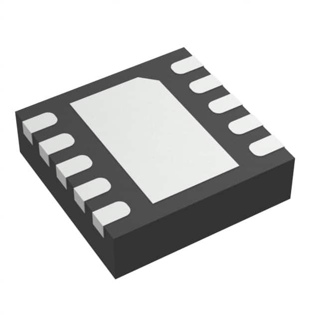
Electronic Components IC Chips Integrated Circuits IC TPS74701QDRCRQ1 one spot buy

Product Attributes
| TYPE | DESCRIPTION |
| Category | Integrated Circuits (ICs) |
| Mfr | Texas Instruments |
| Series | Automotive, AEC-Q100 |
| Package | Tape & Reel (TR)
Cut Tape (CT) Digi-Reel® |
| Product Status | Active |
| Output Configuration | Positive |
| Output Type | Adjustable |
| Number of Regulators | 1 |
| Voltage - Input (Max) | 5.5V |
| Voltage - Output (Min/Fixed) | 0.8V |
| Voltage - Output (Max) | 3.6V |
| Voltage Dropout (Max) | 1.39V @ 500mA |
| Current - Output | 500mA |
| PSRR | 60dB ~ 30dB (1kHz ~ 300kHz) |
| Control Features | Enable, Power Good, Soft Start |
| Protection Features | Over Current, Over Temperature, Short Circuit, Under Voltage Lockout (UVLO) |
| Operating Temperature | -40°C ~ 125°C |
| Mounting Type | Surface Mount |
| Package / Case | 10-VFDFN Exposed Pad |
| Supplier Device Package | 10-VSON (3x3) |
| Base Product Number | TPS74701 |
The relationship between wafers and chips
Overview of wafers
To understand the relationship between wafers and chips, the following is an overview of the key elements of wafer and chip knowledge.
(i) What is a wafer
Wafers are silicon wafers used in the production of silicon semiconductor integrated circuits, which are called wafers because of their circular shape; they can be processed on silicon wafers to form a variety of circuit components and become integrated circuit products with specific electrical functions. The raw material for wafers is silicon, and there is an inexhaustible supply of silicon dioxide on the surface of the earth's crust. Silicon dioxide ore is refined in electric arc furnaces, chlorinated with hydrochloric acid and distilled to produce a high purity polysilicon with a purity of 99.99999999999%.
(ii) Basic raw materials for wafers
Silicon is refined from quartz sand and wafers are purified (99.999%) from the element silicon, which is then made into silicon rods that become the material for quartz semiconductors for integrated circuits.
(iii) Wafer manufacturing process
Wafers are the basic material for manufacturing semiconductor chips. The most important raw material for semiconductor integrated circuits is silicon and therefore corresponds to silicon wafers.
Silicon is widely found in nature in the form of silicates or silicon dioxide in rocks and gravels. The manufacture of silicon wafers can be summarised in three basic steps: silicon refining and purification, single crystal silicon growth, and wafer forming.
The first is silicon purification, where the raw material of sand and gravel is put into an electric arc furnace at a temperature of about 2000 °C and in the presence of a carbon source. At high temperatures, the carbon and the silicon dioxide in the sand and gravel undergo a chemical reaction (carbon combines with oxygen, leaving silicon) to obtain pure silicon with a purity of about 98%, also known as metallurgical grade silicon, which is not pure enough for microelectronic devices because the electrical properties of semiconductor materials are very sensitive to the concentration of impurities. Metallurgical grade silicon is therefore further purified: the crushed metallurgical grade silicon is subjected to a chlorination reaction with gaseous hydrogen chloride to produce liquid silane, which is then distilled and chemically reduced by a process that yields high-purity polycrystalline silicon with a purity of 99.99999999999%, which becomes electronic grade silicon.
Next comes monocrystalline silicon growth, the most common method called direct pulling (CZ method). As shown in the diagram below, high-purity polysilicon is placed in a quartz crucible and heated continuously with a graphite heater surrounding the outside, maintaining the temperature at approximately 1400 °C. The gas in the furnace is usually inert, allowing the polysilicon to melt without creating unwanted chemical reactions. To form single crystals, the orientation of the crystals is also controlled: the crucible is rotated with the polysilicon melt, a seed crystal is immersed in it, and a drawing rod is carried in the opposite direction while slowly and vertically pulling it upwards from the silicon melt. The melted polysilicon sticks to the bottom of the seed crystal and grows upwards in the direction of the lattice arrangement of the seed crystal.
-

TMS320F28035PNT Microcontrollers IC Chip MUC 32...
-
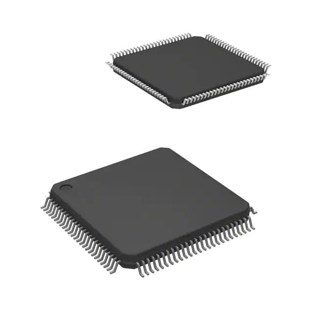
Bom Electronic TMS320F28062PZT IC Chip Integrat...
-
TMS320F28069PZPS Good Price IC Chip Original El...
-

XC7A15T-2CSG325I Artix-7 Field Programmable Gat...
-
.jpg)
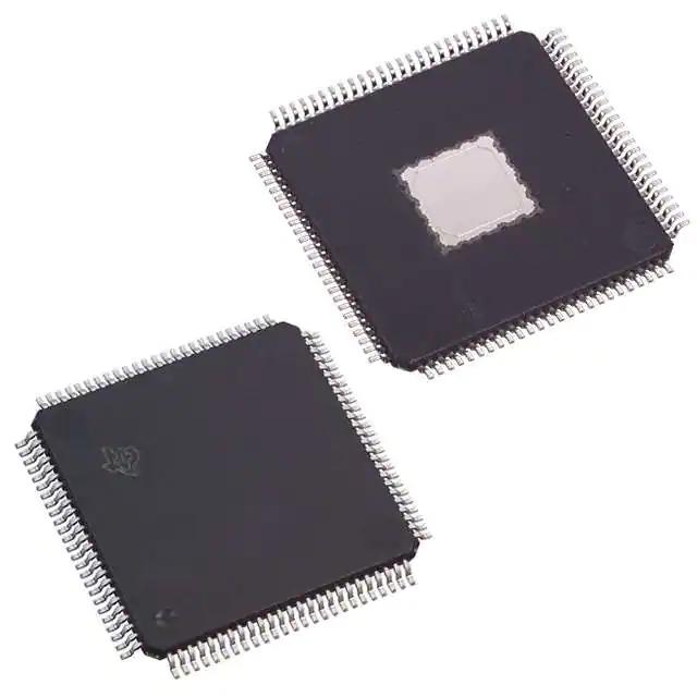
Asourcing hot selling power switch TPS4H160AQPW...
-

10AX048H2F34E2SG 100% New & Original Own S...