CDCLVC1104PWR100% New & Original Own Stock integrated circuit High-Performance Clock Buffer Family

Product Attributes
|
EU RoHS |
Compliant |
|
ECCN (US) |
EAR99 |
|
Part Status |
Active |
|
HTS |
8542.39.00.01 |
|
SVHC |
Yes |
|
Automotive |
No |
|
PPAP |
No |
|
Type |
Fanout Buffer |
|
Fanout |
1:4 |
|
Number of Outputs per Chip |
4 |
|
Maximum Propagation Delay Time @ Maximum CL (ns) |
2.6@2.5V|2@3.3V |
|
Absolute Propagation Delay Time (ns) |
10 |
|
Input Logic Level |
LVCMOS |
|
Output Logic Level |
LVCMOS |
|
Minimum Operating Supply Voltage (V) |
2.3 |
|
Typical Operating Supply Voltage (V) |
2.5|3.3 |
|
Maximum Operating Supply Voltage (V) |
3.6 |
|
Minimum Operating Temperature (°C) |
-40 |
|
Maximum Operating Temperature (°C) |
85 |
|
Packaging |
Tape and Reel |
|
Mounting |
Surface Mount |
Product Introduction
CDCLVC11xx family of clock buffers is designed to serve a broad range of applications including general communications, industrial and consumer applications. With their advanced features and high performance, these clock buffers are sure to be the first choice of electronic engineers and designers.
The CDCLVC11xx family offers powerful features that make it an ideal solution for a wide variety of communication systems. Whether you are working on networking equipment or data center applications, our clock buffers ensure reliable and precise clock distribution. These devices efficiently distribute clock signals with low skew and jitter, ensuring optimal synchronization of all components in the system.
Industrial applications require excellent performance and reliability, and our CDCLVC11xx family delivers exactly that. Whether you are designing test and measurement equipment or factory automation systems, our clock buffers provide high-speed clock distribution with minimal signal degradation. You can rely on the stable and accurate clock signals generated by our devices to ensure seamless operation and precise timing in industrial applications.
Consumer electronics often require high-speed clock distribution for multimedia devices, game consoles, or home entertainment systems. With the CDCLVC11xx family, you can achieve efficient clock distribution and reduce power consumption. These clock buffers support LVCMOS signal levels, making them suitable for a variety of consumer electronics applications. Whether you're doing audio/video synchronization or data transfer, our clock buffers can handle the task with precision and efficiency.
One of the key advantages of the CDCLVC11xx family is that it is compatible with 3.3V and 2.5V signal levels. This feature allows these clock buffers to be seamlessly integrated into existing designs, reducing time-to-market and design complexity. The flexibility to operate at different voltage levels ensures compatibility with a wide range of electronic components, making it a versatile solution for any application.
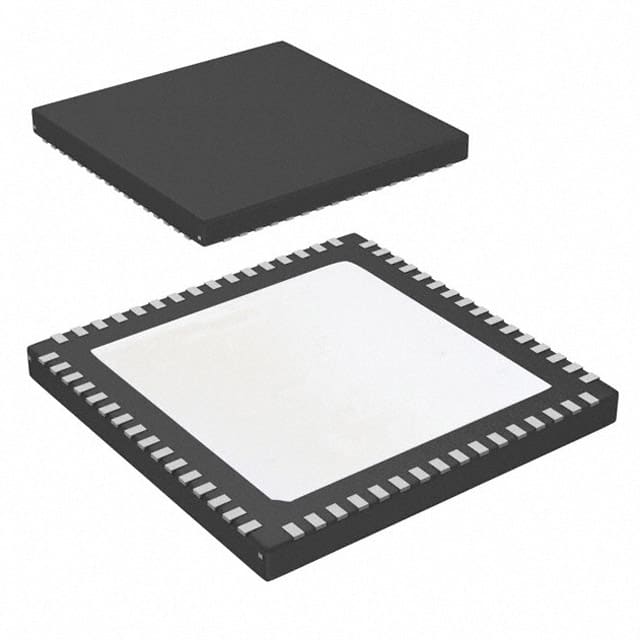
The CDCLVC11xx family is also available in a variety of packaging options, including small packages such as QFN and TSSOP. This makes your design easy to integrate and saves space, important factors for modern electronic devices.
In summary, the CDCLVC11xx 3.3V and 2.5V LVCMOS high-performance clock buffer family is a reliable and efficient solution for a wide variety of applications. Whether you are working on general purpose communication systems, industrial equipment or consumer electronics, our clock buffers provide superior performance, precise timing and reduced power consumption. With compatibility with multiple voltage levels and a variety of packaging options, these clock buffers provide the versatility and convenience that engineers and designers are looking for. Trust the CDCLVC11xx family to enhance the performance and reliability of your electronic systems.