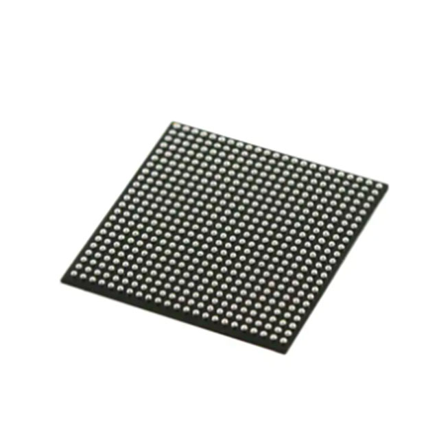
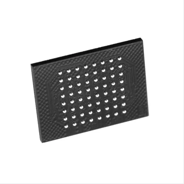
XCF128XFTG64C Encapsulation BGA64 XL high-density configuration and storage devices
Product Attributes
| TYPE | DESCRIPTION |
| Category | Integrated Circuits (ICs) |
| Mfr | AMD Xilinx |
| Series | - |
| Package | Tray |
| Product Status | Obsolete |
| Programmable Type | In System Programmable |
| Memory Size | 128Mb |
| Voltage – Supply | 1.7V ~ 2V |
| Operating Temperature | -40°C ~ 85°C |
| Mounting Type | Surface Mount |
| Package / Case | 64-TBGA |
| Supplier Device Package | 64-FTBGA (10×13) |
| Base Product Number | XCF128 |
Documents & Media
| RESOURCE TYPE | LINK |
| Datasheets | XCF128XFT(G)64C Datasheet |
| Environmental Information | Xiliinx RoHS Cert |
| PCN Obsolescence/ EOL | Multiple Devices 01/Jun/2015 |
| PCN Part Status Change | Parts Reactivated 25/Apr/2016 |
| HTML Datasheet | XCF128XFT(G)64C Datasheet |
Environmental & Export Classifications
| ATTRIBUTE | DESCRIPTION |
| RoHS Status | ROHS3 Compliant |
| Moisture Sensitivity Level (MSL) | 3 (168 Hours) |
| REACH Status | REACH Unaffected |
| ECCN | 3A991B1A |
| HTSUS | 8542.32.0071 |
Xilinx introduces the XC18V00 series of in-system programmable configuration PROMs (Figure 1). Devices in this 3.3V family include a 4-megabit, a 2-megabit, a 1-megabit, and a 512-kilobit PROM that provide an easy-touse, cost-effective method for reprogramming and storing Xilinx FPGA configuration bitstreams.
When the FPGA is in Master Serial mode, it generates a configuration clock that drives the PROM. A short access time after CE and OE are enabled, data is available on the PROM DATA (D0) pin that is connected to the FPGA DIN pin. New data is available a short access time after each rising clock edge. The FPGA generates the appropriate number of clock pulses to complete the configuration. When the FPGA is in Slave Serial mode, the PROM and the FPGA are clocked by an external clock.
When the FPGA is in Master Select MAP mode, the FPGA generates a configuration clock that drives the PROM. When the FPGA is in Slave Parallel or Slave Select MAP mode, an external oscillator generates the configuration clock that drives the PROM and the FPGA. After CE and OE are enabled, data is available on the PROM’s DATA (D0-D7) pins. New data is available a short access time after each rising clock edge. The data is clocked into the FPGA on the following rising edge of the CCLK. A free-running oscillator can be used in the Slave Parallel or Slave Select MAP modes.
Multiple devices can be cascaded by using the CEO output to drive the CE input of the following device. The clock inputs and the DATA outputs of all PROMs in this chain are interconnected. All devices are compatible and can be cascaded with other members of the family or with the XC17V00 one-time programmable serial PROM family.