


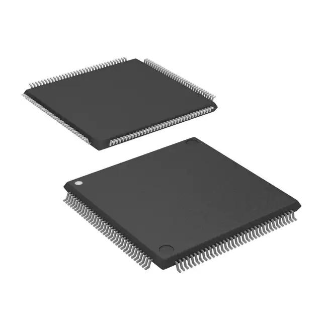
New and original LCMXO2-2000HC-4TG144C Integrated circuit
Product Attributes
| TYPE | DESCRIPTION |
| Category | Integrated Circuits (ICs)Embedded - FPGAs (Field Programmable Gate Array) |
| Mfr | Lattice Semiconductor Corporation |
| Series | MachXO2 |
| Package | Tray |
| Product Status | Active |
| Number of LABs/CLBs | 264 |
| Number of Logic Elements/Cells | 2112 |
| Total RAM Bits | 75776 |
| Number of I/O | 111 |
| Voltage - Supply | 2.375V ~ 3.465V |
| Mounting Type | Surface Mount |
| Operating Temperature | 0°C ~ 85°C (TJ) |
| Package / Case | 144-LQFP |
| Supplier Device Package | 144-TQFP (20x20) |
| Base Product Number | LCMXO2-2000 |
| SPQ | 60/pcs |
Introduction
Field programmable gate array, which is the product of further development on the basis of programmable devices such as PAL, GAL, CPLD and so on. It appears as a semi-custom circuit in the field of application-specific integrated circuits (ASICs), which not only solves the shortcomings of custom circuits, but also overcomes the shortcomings of the limited number of original programmable device gate circuits.
Working Principle
The FPGA adopts a new concept of logic cell array LCA (Logic Cell Array), which includes three parts: configurable logic module CLB, output input module IOB (Input Output Block) and internal connection (Interconnect). The basic features of FPGAs are:
1) Using FPGA to design ASIC circuits, users do not need to produce chips to get a suitable chip.
2) The FPGA can be used as a pilot specimen of other fully customized or semi-customized ASIC circuits.
3) The FPGA has a wealth of flip-flops and I/O pins inside.
4) The FPGA is one of the devices with the shortest design cycle, the lowest development cost and the lowest risk in the ASIC circuit.
5) The FPGA adopts high-speed CHMOS process, low power consumption, and can be compatible with CMOS and TTL levels.
It can be said that FPGA chips are one of the best choices for small batch systems to improve system integration and reliability.
The FPGA is programmed by a program stored in the on-chip RAM to set its operating state, so the on-chip RAM needs to be programmed when working. Users can use different programming methods according to different configuration modes.
When power-on, the FPGA chip reads the data from the EPROM into the on-chip programming RAM, and after the configuration is completed, the FPGA enters the working state. After the power is lost, the FPGA returns to white sheets, and the internal logical relationship disappears, so the FPGA can be used repeatedly. FPGA programming does not require a dedicated FPGA programmer, only a general-purpose EPROM and PROM programmer. When you need to modify the FPGA function, just change the EPROM. In this way, the same FPGA, different programming data, can produce different circuit functions. Therefore, the use of FPGAs is very flexible.
Configuration Modes
The FPGA has a variety of configuration modes: the parallel main mode is a FPGA plus an EPROM; Master-slave mode can support one PIECE PROM programming multiple FPGAs; Serial mode can be programmed with serial PROM FPGA; Peripheral mode allows the FPGA to be used as a peripheral of a microprocessor, programmed by the microprocessor.
Issues such as achieving rapid timing closure, reducing power consumption and cost, optimizing clock management, and reducing the complexity of FPGA and PCB designs have always been key issues for system design engineers using FPGAs. Today, as FPGAs move toward higher density, greater capacity, lower power consumption, and more IP integration, system design engineers benefit from these superior performances while facing new design challenges due to the unprecedented levels of performance and capability of FPGAs.
-
New Original XC7Z015-1CLG485C Inventory Spot Ic...
-
XC7K160T New and Original Electronic Components...
-
BFS481H6327 Integrated Circuits Current Regulat...
-
LMV358IDR Support BOM New&Original IC Inte...
-

Electronic Components IC Chips Integrated Circu...
-
Integrated circuit EP2AGX45DF29C6G Electronic C...