Brand new genuine original IC stock Electronic Components Ic Chip Support BOM Service TPS62130AQRGTRQ1

Product Attributes
| TYPE | DESCRIPTION |
| Category | Integrated Circuits (ICs) |
| Mfr | Texas Instruments |
| Series | Automotive, AEC-Q100, DCS-Control™ |
| Package | Tape & Reel (TR)
Cut Tape (CT) Digi-Reel® |
| SPQ | 250T&R |
| Product Status | Active |
| Function | Step-Down |
| Output Configuration | Positive |
| Topology | Buck |
| Output Type | Adjustable |
| Number of Outputs | 1 |
| Voltage - Input (Min) | 3V |
| Voltage - Input (Max) | 17V |
| Voltage - Output (Min/Fixed) | 0.9V |
| Voltage - Output (Max) | 6V |
| Current - Output | 3A |
| Frequency - Switching | 2.5MHz |
| Synchronous Rectifier | Yes |
| Operating Temperature | -40°C ~ 125°C (TJ) |
| Mounting Type | Surface Mount |
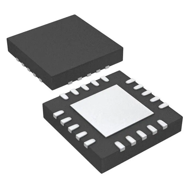
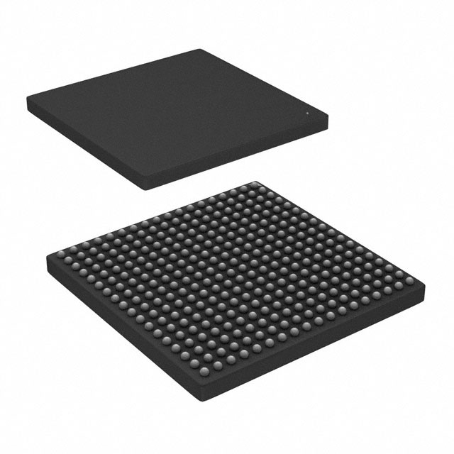
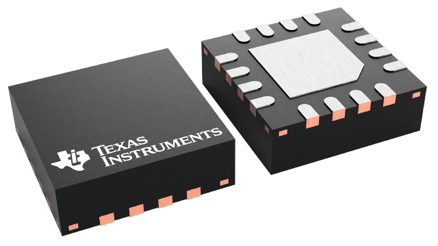
| Package / Case | 16-VFQFN Exposed Pad |
| Supplier Device Package | 16-VQFN (3x3) |
| Base Product Number | TPS62130 |
1.
Once we know how the IC is constructed, it is time to explain how to make it. To make a detailed drawing with a spray can of paint, we need to cut out a mask for the drawing and place it on paper. Then we spray the paint evenly onto the paper and remove the mask when the paint has dried. This is repeated over and over again to create a neat and complex pattern. I am made similarly, by stacking layers on top of each other in a masking process.
The production of ICs can be divided into these 4 simple steps. Although the actual manufacturing steps may vary and the materials used may differ, the general principle is similar. The process is slightly different from painting, in that ICs are manufactured with paint and then masked, whereas paint is first masked and then painted. Each process is described below.
Metal sputtering: The metal material to be used is evenly sprinkled on the wafer to form a thin film.
Photoresist application: The photoresist material is first placed on the wafer, and through the photomask (the principle of the photomask will be explained next time), the light beam is hit on the unwanted part to destroy the structure of the photoresist material. The damaged material is then washed away with chemicals.
Etching: The silicon wafer, which is not protected by the photoresist, is etched with an ion beam.
Photoresist removal: The remaining photoresist is dissolved using a photoresist removal solution, thus completing the process.
The final result is several 6IC chips on a single wafer, which are then cut out and sent to the packaging plant for packaging.
2.What is the nanometer process?
Samsung and TSMC are fighting it out in the advanced semiconductor process, each trying to get a head start in the foundry to secure orders, and it has almost become a battle between 14nm and 16nm. And what are the benefits and problems that will be brought about by the reduced process? Below we will briefly explain the nanometer process.
How small is a nanometre?
Before we start, it is important to understand what nanometres mean. In mathematical terms, a nanometre is 0.000000001 meter, but this is a rather poor example - after all, we can only see several zeros after the decimal point but have no real sense of what they are. If we compare this with the thickness of a fingernail, it might be more obvious.
If we use a ruler to measure the thickness of a nail, we can see that the thickness of a nail is about 0.0001 meter (0.1 mm), which means that if we try to cut the side of a nail into 100,000 lines, each line is equivalent to about 1 nanometre.
Once we know how small a nanometre is, we need to understand the purpose of shrinking the process. The main purpose of shrinking the crystal is to fit more crystals into a smaller chip so that the chip will not become larger due to technological advancement. Finally, the reduced size of the chip will make it easier to fit into mobile devices and meet future demand for thinness.
Taking 14nm as an example, the process refers to the smallest possible wire size of 14nm in a chip.