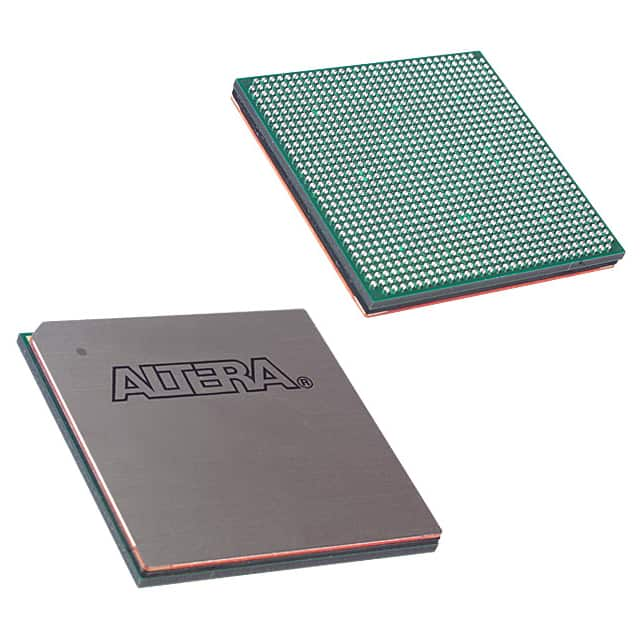
XC7Z015-2CLG485I – Integrated Circuits (ICs), Embedded, System On Chip (SoC)
Product Attributes
| TYPE | DESCRIPTION |
| Category | Integrated Circuits (ICs) |
| Mfr | AMD |
| Series | Zynq®-7000 |
| Package | Tray |
| Product Status | Active |
| Architecture | MCU, FPGA |
| Core Processor | Dual ARM® Cortex®-A9 MPCore™ with CoreSight™ |
| Flash Size | - |
| RAM Size | 256KB |
| Peripherals | DMA |
| Connectivity | CANbus, EBI/EMI, Ethernet, I²C, MMC/SD/SDIO, SPI, UART/USART, USB OTG |
| Speed | 766MHz |
| Primary Attributes | Artix™-7 FPGA, 74K Logic Cells |
| Operating Temperature | -40°C ~ 100°C (TJ) |
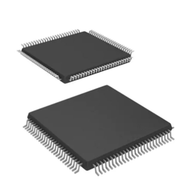
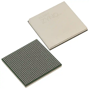
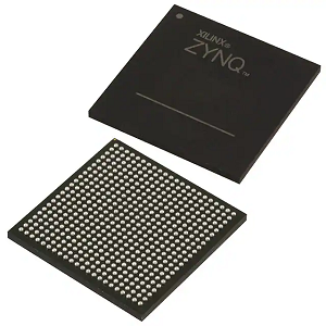
| Package / Case | 485-LFBGA, CSPBGA |
| Supplier Device Package | 485-CSPBGA (19x19) |
| Number of I/O | 130 |
| Base Product Number | XC7Z015 |
Documents & Media
| RESOURCE TYPE | LINK |
| Datasheets | Zynq-7000 SoC Specification |
| Environmental Information | Xiliinx RoHS Cert |
| Featured Product | All Programmable Zynq®-7000 SoC |
| EDA Models | XC7Z015-2CLG485I by Ultra Librarian |
Environmental & Export Classifications
| ATTRIBUTE | DESCRIPTION |
| RoHS Status | ROHS3 Compliant |
| Moisture Sensitivity Level (MSL) | 3 (168 Hours) |
| REACH Status | REACH Unaffected |
| ECCN | 3A991A2 |
| HTSUS | 8542.39.0001 |
PL Power‐On/Off Power Supply Sequencing
The recommended power-on sequence for the PL is VCCINT, VCCBRAM, VCCAUX, and VCCO to achieve minimum current draw and ensure that the I/Os are 3-stated at power-on. The recommended power-off sequence is the reverse of the power-on sequence. If VCCINT and VCCBRAM have the same recommended voltage levels then both can be powered by the same supply and ramped simultaneously. If VCCAUX and VCCO have the same recommended voltage levels then both can be powered by the same supply and ramped simultaneously.
For VCCO voltages of 3.3V in HR I/O banks and configuration bank 0:
• The voltage difference between VCCO and VCCAUX must not exceed 2.625V for longer than TVCCO2VCCAUX for each power-on/off cycle to maintain device reliability levels.
• The TVCCO2VCCAUX time can be allocated in any percentage between the power-on and power-off ramps.
GTP Transceivers (XC7Z012S and XC7Z015 Only)
The recommended power-on sequence to achieve minimum current draw for the GTP transceivers (XC7Z012S and XC7Z015 only) is VCCINT, VMGTAVCC, VMGTAVTT OR VMGTAVCC, VCCINT, VMGTAVTT. Both VMGTAVCC and VCCINT can be ramped simultaneously. The recommended power-off sequence is the reverse of the power-on sequence to achieve minimum current draw.
If these recommended sequences are not met, current drawn from VMGTAVTT can be higher than specifications during power-up and power-down.
• When VMGTAVTT is powered before VMGTAVCC and VMGTAVTT – VMGTAVCC > 150 mV and VMGTAVCC < 0.7V, the VMGTAVTT current draw can increase by 460 mA per transceiver during VMGTAVCC ramp up. The duration of the current draw can be up to 0.3 x TMGTAVCC (ramp time from GND to 90% of VMGTAVCC). The reverse is true for power-down.
• When VMGTAVTT is powered before VCCINT and VMGTAVTT – VCCINT > 150 mV and VCCINT < 0.7V, the VMGTAVTT current draw can increase by 50 mA per transceiver during VCCINT ramp up. The duration of the current draw can be up to 0.3 x TVCCINT (ramp time from GND to 90% of VCCINT). The reverse is true for power-down.
There is no recommended sequence for supplies not shown.