


New Original Integrated Circuit Chip IC DS90UB928QSQX/NOPB

Product Attributes
| TYPE | DESCRIPTION |
| Category | Integrated Circuits (ICs)Interface - Serializers, Deserializers |
| Mfr | Texas Instruments |
| Series | Automotive, AEC-Q100 |
| Package | Tape & Reel (TR)Cut Tape (CT)
Digi-Reel® |
| Part Status | Active |
| Function | Deserializer |
| Data Rate | 2.975Gbps |
| Input Type | FPD-Link III, LVDS |
| Output Type | LVDS |
| Number of Inputs | 1 |
| Number of Outputs | 13 |
| Voltage - Supply | 3V ~ 3.6V |
| Operating Temperature | -40°C ~ 105°C (TA) |
| Mounting Type | Surface Mount |
| Package / Case | 48-WFQFN Exposed Pad |
| Supplier Device Package | 48-WQFN (7x7) |
| Base Product Number | DS90UB928 |
Wafer manufacturing
The original material of the chip is sand, which is the magic of science and technology. The main component of sand is silicon dioxide (SiO2), and deoxidized sand contains up to 25 percent silicon, the second most abundant element in the earth's crust and the basis of the semiconductor manufacturing industry.
Sand smelting and multi-step purification and purification can be used for semiconductor manufacturing of high-purity polysilicon, known as electron grade silicon, on average there is only one impurity atom in a million silicon atoms. 24-karat gold, as you all know, is 99.998% pure, but not as pure as electronic-grade silicon.
High purity polysilicon in the single crystal furnace pulling, you can get nearly cylindrical single crystal silicon ingot, weight of about 100 kg, silicon purity up to 99.9999%. The Wafer is called Wafer, which is usually used to make chips, by cutting single crystal silicon ingots horizontally into round single silicon wafers.
Monocrystalline silicon is better than polycrystalline silicon in electrical and mechanical properties, so semiconductor manufacturing is based on monocrystalline silicon as the basic material.
An example from life can help you understand polysilicon and monocrystalline silicon. Rock candy we should have seen, childhood often eat like square ice cubes like rock candy, in fact, is a single crystal rock candy. The corresponding polycrystalline rock candy, usually irregular in shape, is used in traditional Chinese medicine or soup, which has the effect of moistening lung and relieving cough.
The same material crystal arrangement structure is different, its performance and use will be different, even obvious difference.
Semiconductor manufacturers, factories that do not normally produce wafers but merely move wafers, buy wafers directly from Wafer suppliers.
Wafer fabrication is all about putting designed circuits (called masks) on wafers.
First, we need to evenly spread the photoresist on the wafer surface. During this process, we need to keep the wafer rotating so that the photoresist can be spread very thin and flat. The photoresist layer is then exposed to ultraviolet light (UV) through a Mask and becomes soluble.
The mask is printed with a pre-designed circuit pattern, through which ultraviolet light shines on the photoresist layer, forming each layer of the circuit pattern. Typically, the circuit pattern you get on a wafer is a quarter of the pattern you get on the mask.
The end result is somewhat similar. Photolithography takes the circuitry of the design and implements it on a wafer, resulting in a chip, just as a photograph takes a picture and implements what the real thing looks like on film.
Photolithography is one of the most important processes in chip manufacturing. With photolithography, we can lay the designed circuit on a wafer, and repeat this process to create multiple identical circuits on the wafer, each of which is a separate chip, called die. The actual chip-making process is much more complex than that, usually involving hundreds of steps. So semiconductors are the crown of manufacturing.
Understanding the chip manufacturing process is very important for positions related to semiconductor manufacturing, especially for technicians in FAB plants or mass production positions such as product engineer and test engineer in chip r&d teams.
-
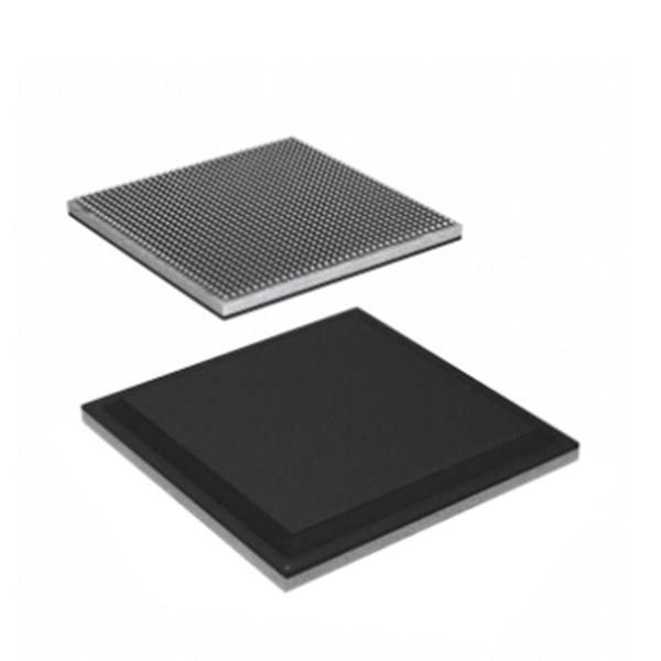
AQX XCKU040-2FFVA1156I New and original integra...
-
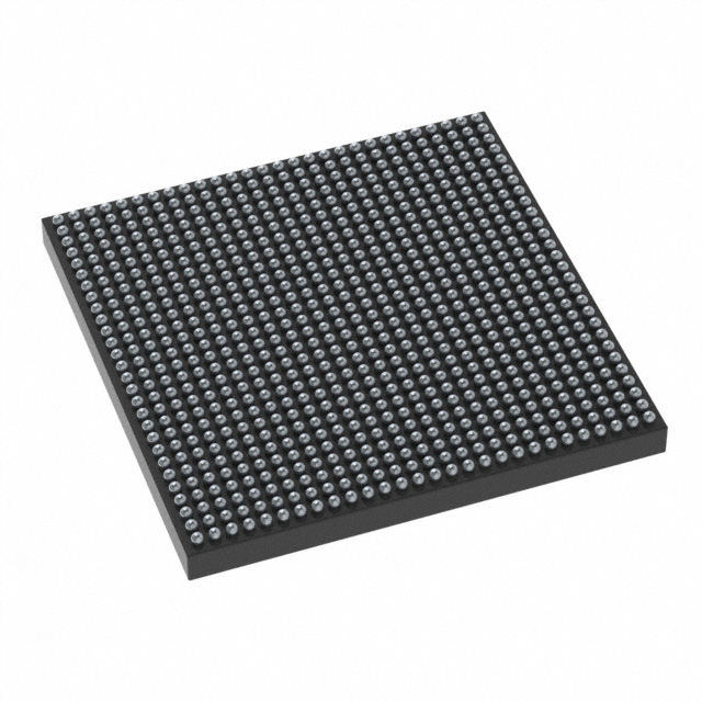
Hot offer Ic chip (Electronic Components IC Sem...
-

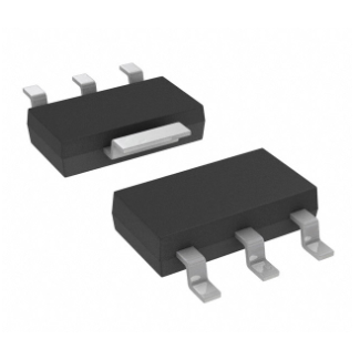
one-stop shop for electronic components TLV1117...
-
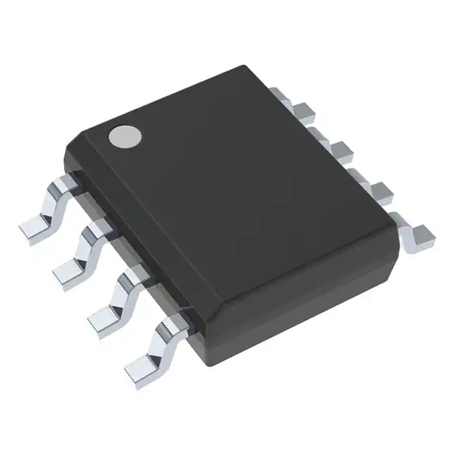
Original New In Stock MOSFET Transistor Diode T...
-
.png)
DS90UB936TRGZTQ1 48-VQFN-EP (7×7) integrat...
-
Electronic Components IC Chips Integrated Circu...