


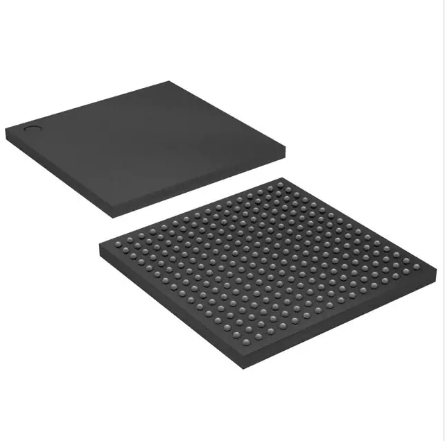
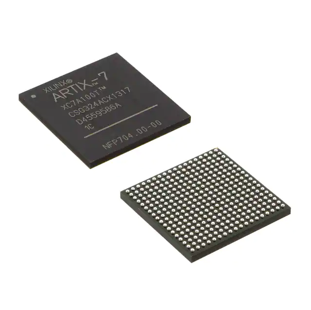
(New & Original) In stock 3S200A-4FTG256C IC Chip XC3S200A-4FTG256C
Product Attributes
| TYPE | DESCRIPTION |
SELECT |
| Category | Integrated Circuits (ICs) |
|
| Mfr | AMD Xilinx |
|
| Series | Spartan®-3A |
|
| Package | Tray |
|
| Product Status | Active |
|
| Number of LABs/CLBs | 448 |
|
| Number of Logic Elements/Cells | 4032 |
|
| Total RAM Bits | 294912 |
|
| Number of I/O | 195 |
|
| Number of Gates | 200000 |
|
| Voltage – Supply | 1.14V ~ 1.26V |
|
| Mounting Type | Surface Mount |
|
| Operating Temperature | 0°C ~ 85°C (TJ) |
|
| Package / Case | 256-LBGA |
|
| Supplier Device Package | 256-FTBGA (17×17) |
|
| Base Product Number | XC3S200 |
Field Programmable Gate Array
A field-programmable gate array (FPGA) is an integrated circuit designed to be configured by a customer or a designer after manufacturing – hence the term field-programmable. The FPGA configuration is generally specified using a hardware description language (HDL), similar to that used for an application-specific integrated circuit (ASIC). Circuit diagrams were previously used to specify the configuration, but this is increasingly rare due to the advent of electronic design automation tools.
FPGAs contain an array of programmable logic blocks, and a hierarchy of reconfigurable interconnects allowing blocks to be wired together. Logic blocks can be configured to perform complex combinational functions, or act as simple logic gates like AND and XOR. In most FPGAs, logic blocks also include memory elements, which may be simple flip-flops or more complete blocks of memory.[1] Many FPGAs can be reprogrammed to implement different logic functions, allowing flexible reconfigurable computing as performed in computer software.
FPGAs have a remarkable role in embedded system development due to their capability to start system software development simultaneously with hardware, enable system performance simulations at a very early phase of the development, and allow various system trials and design iterations before finalizing the system architecture.[2]
History[edit]
The FPGA industry sprouted from programmable read-only memory (PROM) and programmable logic devices (PLDs). PROMs and PLDs both had the option of being programmed in batches in a factory or in the field (field-programmable).[3]
Altera was founded in 1983 and delivered the industry’s first reprogrammable logic device in 1984 – the EP300 – which featured a quartz window in the package that allowed users to shine an ultra-violet lamp on the die to erase the EPROM cells that held the device configuration.[4]
Xilinx produced the first commercially viable field-programmable gate array in 1985[3] – the XC2064.[5] The XC2064 had programmable gates and programmable interconnects between gates, the beginnings of a new technology and market.[6] The XC2064 had 64 configurable logic blocks (CLBs), with two three-input lookup tables (LUTs).[7]
In 1987, the Naval Surface Warfare Center funded an experiment proposed by Steve Casselman to develop a computer that would implement 600,000 reprogrammable gates. Casselman was successful and a patent related to the system was issued in 1992.[3]
Altera and Xilinx continued unchallenged and quickly grew from 1985 to the mid-1990s when competitors sprouted up, eroding a significant portion of their market share. By 1993, Actel (now Microsemi) was serving about 18 percent of the market.[6]
The 1990s were a period of rapid growth for FPGAs, both in circuit sophistication and the volume of production. In the early 1990s, FPGAs were primarily used in telecommunications and networking. By the end of the decade, FPGAs found their way into consumer, automotive, and industrial applications.[8]
By 2013, Altera (31 percent), Actel (10 percent) and Xilinx (36 percent) together represented approximately 77 percent of the FPGA market.[9]
Companies like Microsoft have started to use FPGAs to accelerate high-performance, computationally intensive systems (like the data centers that operate their Bing search engine), due to the performance per watt advantage FPGAs deliver.[10] Microsoft began using FPGAs to accelerate Bing in 2014, and in 2018 began deploying FPGAs across other data center workloads for their Azure cloud computing platform.[11]
The following timelines indicate progress in different aspects of FPGA design:
Gates
- 1987: 9,000 gates, Xilinx[6]
- 1992: 600,000, Naval Surface Warfare Department[3]
- Early 2000s: millions[8]
- 2013: 50 million, Xilinx[12]
Market size
- 1985: First commercial FPGA : Xilinx XC2064[5][6]
- 1987: $14 million[6]
- c. 1993: >$385 million[6][failed verification]
- 2005: $1.9 billion[13]
- 2010 estimates: $2.75 billion[13]
- 2013: $5.4 billion[14]
- 2020 estimate: $9.8 billion[14]
Design starts
A design start is a new custom design for implementation on an FPGA.
Design[edit]
Contemporary FPGAs have large resources of logic gates and RAM blocks to implement complex digital computations. As FPGA designs employ very fast I/O rates and bidirectional data buses, it becomes a challenge to verify correct timing of valid data within setup time and hold time.
Floor planning enables resource allocation within FPGAs to meet these time constraints. FPGAs can be used to implement any logical function that an ASIC can perform. The ability to update the functionality after shipping, partial re-configuration of a portion of the design[17] and the low non-recurring engineering costs relative to an ASIC design (notwithstanding the generally higher unit cost), offer advantages for many applications.[1]
Some FPGAs have analog features in addition to digital functions. The most common analog feature is a programmable slew rate on each output pin, allowing the engineer to set low rates on lightly loaded pins that would otherwise ring or couple unacceptably, and to set higher rates on heavily loaded pins on high-speed channels that would otherwise run too slowly.[18][19] Also common are quartz-crystal oscillators, on-chip resistance-capacitance oscillators, and phase-locked loops with embedded voltage-controlled oscillators used for clock generation and management as well as for high-speed serializer-deserializer (SERDES) transmit clocks and receiver clock recovery. Fairly common are differential comparators on input pins designed to be connected to differential signaling channels. A few “mixed signal FPGAs” have integrated peripheral analog-to-digital converters (ADCs) and digital-to-analog converters (DACs) with analog signal conditioning blocks allowing them to operate as a system-on-a-chip (SoC).[20] Such devices blur the line between an FPGA, which carries digital ones and zeros on its internal programmable interconnect fabric, and field-programmable analog array (FPAA), which carries analog values on its internal programmable interconnect fabric.
Logic blocks[edit]
Main article: Logic block
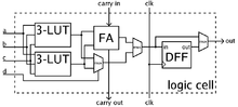
Simplified example illustration of a logic cell (LUT – Lookup table, FA – Full adder, DFF – D-type flip-flop)
The most common FPGA architecture consists of an array of logic blocks (called configurable logic blocks, CLBs, or logic array blocks, LABs, depending on vendor), I/O pads, and routing channels.[1] Generally, all the routing channels have the same width (number of wires). Multiple I/O pads may fit into the height of one row or the width of one column in the array.
“An application circuit must be mapped into an FPGA with adequate resources. While the number of CLBs/LABs and I/Os required is easily determined from the design, the number of routing tracks needed may vary considerably even among designs with the same amount of logic. (For example, a crossbar switch requires much more routing than a systolic array with the same gate count. Since unused routing tracks increase the cost (and decrease the performance) of the part without providing any benefit, FPGA manufacturers try to provide just enough tracks so that most designs that will fit in terms of lookup tables (LUTs) and I/Os can be routed. This is determined by estimates such as those derived from Rent’s rule or by experiments with existing designs.”[21] As of 2018, network-on-chip architectures for routing and interconnection are being developed.[citation needed]
In general, a logic block consists of a few logical cells (called ALM, LE, slice etc.). A typical cell consists of a 4-input LUT, a full adder (FA) and a D-type flip-flop. These might be split into two 3-input LUTs. In normal mode those are combined into a 4-input LUT through the first multiplexer (mux). In arithmetic mode, their outputs are fed to the adder. The selection of mode is programmed into the second mux. The output can be either synchronous or asynchronous, depending on the programming of the third mux. In practice, entire or parts of the adder are stored as functions into the LUTs in order to save space.[22][23][24]
Hard blocks[edit]
Modern FPGA families expand upon the above capabilities to include higher level functionality fixed in silicon. Having these common functions embedded in the circuit reduces the area required and gives those functions increased speed compared to building them from logical primitives. Examples of these include multipliers, generic DSP blocks, embedded processors, high speed I/O logic and embedded memories.
Higher-end FPGAs can contain high speed multi-gigabit transceivers and hard IP cores such as processor cores, Ethernet medium access control units, PCI/PCI Express controllers, and external memory controllers. These cores exist alongside the programmable fabric, but they are built out of transistors instead of LUTs so they have ASIC-level performance and power consumption without consuming a significant amount of fabric resources, leaving more of the fabric free for the application-specific logic. The multi-gigabit transceivers also contain high performance analog input and output circuitry along with high-speed serializers and deserializers, components which cannot be built out of LUTs. Higher-level physical layer (PHY) functionality such as line coding may or may not be implemented alongside the serializers and deserializers in hard logic, depending on the FPGA.
-
ADG1419BRMZ-REEL7 Diode Transistors Electronics...
-

TMS320F28035PNT Microcontrollers IC Chip MUC 32...
-
Original New In Stock MOSFET Transistor Diode T...
-
In Stock Original Electronic Component IC Chip ...
-
JXSQ New and Original IC chips REG BUCK ADJ 3.5...
-
STF13N80K5 Trans MOSFET N-CH 800V 12A 3-Pin(3+T...